Features: . Binary/2's comp output format
. Single supply operation
. Internal sample-and-hold
. Outputs 2.5V to 5V compatible
. TTL/CMOS compatible input/outputs
. Low power consumption
. Power down mode
. On-chip reference buffer
. Internal/External 2v referenceApplication. UltrasoundandImaging
. Instrumentation
. CommunicationsReceivers
. Sonar/Radar
. xDSL
. CableModems
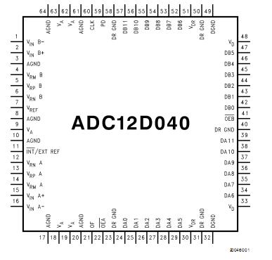
. DSPFrontEndsPinout Specifications
If Military/Aerospace specified devices are required, please contact the National Semiconductor Sales Office/Distributors for a vailability and specifications.
VA, VD, VDR ................................................................6.5V
VDR VD.....................................................................+0.3V
|VAVD|............................................................... 100mV
Voltage on Any Input or Output Pin...... −0.3V to VA or VD
+0.3V
Input Current at AnyPin(Note3)............................ ±25mA
Package Input Current (Note3) .............................±50mA
Package Dissipation at TA=25˚C..................... See(Note4)
ESD Susceptibility
Human Body Model (Note5).................................... 2500V
Machine Model (Note5)............................................. 250V
Soldering Temperature,
Infrared, 10sec. (Note6) ..........................................235˚C
Storage Temperature ...............................−65˚C to+150˚C
DescriptionThe ADC12D040 is adual, low power monolithic CMOS analog-to-digital converter capable of converting analog input signals into 12-bit digital words at 40 Megasamples per second (MSPS), minimum. This converter uses a differential, pipe line darchitecture with digital error correction and anon-chip sample-and-hold circuit to minimize die size and power consumption while providing excellent dynamic per-formance. Operating on a single 5V power supply,the ADC12D040 achieves 10.9 effective bits at 10MHz input and consumes just 600mW at 40MSPS, including the reference current.The Power Down feature reduces power consumption to 75mW.
The differential inputs provide a full scale input swing equal to VREF with the possibility of a single-ended input.Full use of the differential input is recommended for optimum perfor-mance. For ease of use,the buffered, high impedance, single-ended reference input is converted on-chip to a differ-ential reference for use by the processing circuitry.The digital outputs for the two ADC sare available on separate 12-bit buses with an outputd at a format choice of offset binary or 2's complement.
For ease of interface,the digital output driver power pin soft he ADC12D040 can be connected to aseparatesupply voltage in the range of 2.5V to the digital supply voltage, making the outputs compatible with low voltagesystems. When not converting, power consumption can be reduced by pulling the PD pin high, placing the converter into the power down state where it typically consumes just 75 mW. The ADC12D040's speed, resolution and single supply operation makeit well suited for a variety of applications.
This device ADC12D040 is available in the 64-lead TQFP package and will operate over the industrial temperature range of −40˚C to +85˚C.

 ADC12D040 Data Sheet


