PinoutSpecificationsResolution10 bitsChannels2 ChannelsSNR61 dBSFDR85 dBENOB9.8 bitsMax Sample Rate65 MSPSMin Sample Rate15 MSPSPower Dissipation0.36 WattPowerWise Rating 13.11 pJ/convINL (+/-)0.25 LSBSINAD69.9 dBDNL (+/-)0.4 LSBTHD dB-83.5 dBMin Supply Voltage3 VoltMax Supply Voltage3.6 VoltNomin...
ADC10DL065: PinoutSpecificationsResolution10 bitsChannels2 ChannelsSNR61 dBSFDR85 dBENOB9.8 bitsMax Sample Rate65 MSPSMin Sample Rate15 MSPSPower Dissipation0.36 WattPowerWise Rating 13.11 pJ/convINL (+/-)0.25 ...
SeekIC Buyer Protection PLUS - newly updated for 2013!
268 Transactions
All payment methods are secure and covered by SeekIC Buyer Protection PLUS.
Resolution | 10 bits |
Channels | 2 Channels |
SNR | 61 dB |
SFDR | 85 dB |
ENOB | 9.8 bits |
Max Sample Rate | 65 MSPS |
Min Sample Rate | 15 MSPS |
Power Dissipation | 0.36 Watt |
PowerWise Rating 1 | 3.11 pJ/conv |
INL (+/-) | 0.25 LSB |
SINAD | 69.9 dB |
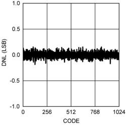
DNL (+/-) | 0.4 LSB |
THD dB | -83.5 dB |
Min Supply Voltage | 3 Volt |
Max Supply Voltage | 3.6 Volt |
Nominal Vin | 2 Vpp |
Temperature Min | -40 deg C |
Temperature Max | 85 deg C |
Data Converter Type | ADC |
Automotive Selection Guide | Yes |
PowerWise | No |
View Using Catalog |
The ADC10DL065 is a dual, low power monolithic CMOS analog-to-digital converter capable of converting analog input signals into 10-bit digital words at 65 Megasamples per second (MSPS). This converter uses a differential, pipeline architecture with digital error correction and an on-chip sample-and-hold circuit to minimize power consumption while providing excellent dynamic performance and a 250 MHz Full Power Bandwidth. Operating on a single +3.3V power supply, the ADC10DL065 achieves 9.8 effective bits at nyquist and consumes just 370 mW at 65 MSPS, including the reference current. The Power Down feature reduces power consumption to 36 mW.
The differential inputs provide a full scale differential input swing equal to 2 times VREF with the possibility of a single-ended input. Full use of the differential input is recommended for optimum performance. The digital outputs from the two ADC's are available on a single multiplexed 10-bit bus or on separate buses. Duty cycle stabilization and output data format are selectable using a quad state function pin. The output data can be set for offset binary or two's complement.
To ease interfacing to lower voltage systems, the digital output driver power pins of the ADC10DL065 can be connected to a separate supply voltage in the range of 2.4V to the analog supply voltage. This device is available in the 64-lead TQFP package and will operate over the industrial temperature range of -40°C to +85°C. An evaluation board is available to ease the evaluation process.
Design Tools
Title | Size in Kbytes | Date | |||
Evaluation Systems | 32 Kbytes | 2-Jun-2008 | View |
If you have trouble printing or viewing PDF file(s), see Printing Problems. |