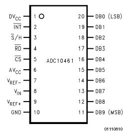
Features: ·Built-in sample-and-hold
·Single +5V supply
·1, 2, or 4-input multiplexer options
·No external clock required
·Speed adjust pin for faster conversions (ADC10462 and ADC10464)Application·Digital signal processor front ends
·Instrumentation
·Disk drives
·Mobile telecommunicationsPinout SpecificationsSupply Voltage (V+ = AVCC = DVCC) -0.3V to +6V
Voltage at Any Input or Output -0.3V to V+ + 0.3V
Input Current at Any Pin (Note 3) 5 mA
Package Input Current (Note 3) 20 mA
Power Dissipation (Note 4) 875 mW
ESD Susceptability (Note 5)2000V
Soldering Information (Note 6)
N Package (10 Sec) 260
SO Package:
Vapor Phase (60 Sec) 215
Infrared (15 Sec) 220
Storage Temperature Range -65 to +150
Junction Temperature 150DescriptionUsing an innovative, patented multistep* conversion technique, the 10-bit ADC10461, ADC10462, and ADC10464 CMOS analog-to-digital converters offer sub-microsecond conversion times yet dissipate a maximum of only 235 mW. The ADC10461, ADC10462, and ADC10464 perform a 10-bit conversion in two lower-resolution "flashes", thus yielding a fast A/D without the cost, power dissipation, and other problems associated with true flash approaches. Dynamic performance (THD, S/N) is guaranteed. The ADC10461 is pin-compatible with the ADC1061 but much faster, thus providing a convenient upgrade path for the ADC1061.
The analog input voltage to the ADC10461, ADC10462, and ADC10464 is sampled and held by an internal sampling circuit. Input signals at frequencies from dc to over 200 kHz can therefore be digitized accurately without the need for an external sample-and-hold circuit.
The ADC10462 and ADC10464 include a "speed-up" pin. Connecting an external resistor between this pin and ground reduces the typical conversion time to as little as 350 ns with only a small increase in linearity error.
For ease of interface to microprocessors, the ADC10461, ADC10462, and ADC10464 have been designed to appear as a memory location or I/O port without the need for external interface logic.

 ADC10461 Data Sheet


