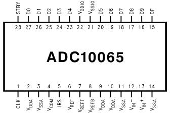
Features: `Single +3.0V operation
`Selectable 2.0 VP-P, 1.5 VP-P, or 1.0 VP-P full-scale input swing
`400 MHz -3 dB input bandwidth
`Low power consumption
`Standby mode
`On-chip reference and sample-and-hold amplifier
`Offset binary or two's complement data format
`Separate adjustable output driver supply to accommodate 2.5V and 3.3V logic families
`28-pin TSSOP package
Application·Ultrasound and Imaging
·Instrumentation
·Cellular Based Stations/Communications Receivers
·Sonar/Radar
·xDSL
·Wireless Local Loops
·Data Acquisition Systems
·DSP Front EndsPinout Specifications
| Resolution |
10 bits |
| Channels |
1 Channels |
| SNR |
59.6 dB |
| SFDR |
80 dB |
| ENOB |
9.6 bits |
| Max Sample Rate |
65 MSPS |
| Min Sample Rate |
20 MSPS |
| Power Dissipation |
0.0684 Watt |
| PowerWise Rating 1 |
1.36 pJ/conv |
| INL (+/-) |
0.3 LSB |
| SINAD |
59.4 dB |
| DNL (+/-) |
0.3 LSB |
| THD dB |
-74 dB |
| Min Supply Voltage |
2.7 Volt |
| Max Supply Voltage |
3.6 Volt |
| Nominal Vin |
1.5 Vpp |
| Temperature Min |
-40 deg C |
| Temperature Max |
85 deg C |
| Data Converter Type |
ADC |
| Automotive Selection Guide |
Yes |
| PowerWise |
Yes |
| View Using Catalog |
VDDA, VDDIO 3.9V
Voltage on Any Pin to GND -0.3V to VDDA or
VDDIO +0.3V
Input Current on Any Pin ±25 mA
Package Input Current (Note 3) ±50 mA
Package Dissipation at T = 25 See (Note 4)
ESD Susceptibility
Human Body Model (Note 5)2500V
Machine Model (Note 5) 250V
Soldering Temperature
Infrared, 10 sec. (Note 6) 235
Storage Temperature -65 to +150
DescriptionThe ADC10065 is a monolithic CMOS analog-to-digital converter capable of converting analog input signals into 10-bit digital words at 65 Megasamples per second (MSPS). This converter uses a differential, pipeline architecture with digital error correction and an on-chip sample-and-hold circuit to provide a complete conversion solution, and to minimize power consumption, while providing excellent dynamic performance. A unique sample-and-hold stage yields a full-power bandwidth of 400 MHz. Operating on a single 3.0V power supply, this device consumes just 68.4 mW at 65 MSPS, including the reference current. The Standby feature reduces power consumption to just 14 .1 mW.
The differential inputs of ADC10065 provide a full scale selectable input swing of 2.0 VP-P, 1.5 VP-P, 1.0 VP-P, with the possibility of a single-ended input. Full use of the differential input is recommended for optimum performance. An internal +1.2V precision bandgap reference is used to set the ADC full-scale range, and also allows the user to supply a buffered referenced voltage for those applications requiring increased accuracy. The output data format is user choice of offset binary or two's complement.
This device ADC10065 is available in the 28-lead TSSOP package and will operate over the industrial temperature range of −40°C to +85°C.
Reliability Metrics
| Part Number |
Process |
EFR Reject |
EFR Sample Size |
PPM |
LTA Rejects |
LTA Device Hours |
FITS |
MTTF (Hours) |
| ADC10065CIMT |
CMOS9 |
1 |
6382 |
157 |
0 |
923000 |
4 |
261903770 |
| ADC10065CIMTX |
CMOS9 |
1 |
6382 |
157 |
0 |
923000 |
4 |
261903770 |
Note: The Early Failure Rates (EFR) were calculated as point estimate PPM based on rejects and sample size for EFR. The Long Term Failure Rates were calculated at 60% confidence using the Arrhenius equation at 0.7eV activation energy and derating the assumed stress temperature of 150°C to an application temperature of 55°C.For more information on Reliability Metrics, please click here.
Design Tools
| Title |
Size in Kbytes |
Date |
|
|
|
| Evaluation Systems |
32 Kbytes |
2-Jun-2008 |
View |
|
|
If you have trouble printing or viewing PDF file(s), see Printing Problems.
|
More Application Notes
| Title |
Size in Kbytes |
Date |
|
| AN-769: Dynamic Specifications for Sampling A/D Converters |
128 Kbytes |
5-Aug-95 |
Download |
If you have trouble printing or viewing PDF file(s), see Printing Problems.
|
The ADC10065 is a monolithic CMOS analog-to-digital converter capable of converting analog input signals into 10-bit digital words at 65 Megasamples per second (MSPS). This converter uses a differential, pipeline architecture with digital error correction and an on-chip sample-and-hold circuit to provide a complete conversion solution, and to minimize power consumption, while providing excellent dynamic performance.
A unique sample-and-hold stage yields a fullpower bandwidth of 400 MHz. Operating on a single 3.0V power supply, this device consumes just 68.4 mW at 65 MSPS, including the reference current. The Standby feature reduces power consumption to just 14 .1 mW.
The differential inputs provide a full scale selectable input swing of 2.0 VP-P, 1.5 VP-P, 1.0 VP-P, with the possibility of a single-ended input. Full use of the differential input is recommended for optimum performance. An internal +1.2V precision bandgap reference is used to set the ADC full-scale range, and also allows the user to supply a buffered referenced voltage for those applications requiring increased accuracy. The output data format is 10-bit offset binary, or two's complement.
This device is available in the 28-lead TSSOP package and will operate over the industrial temperature range of -40 to +85.

 ADC10065 Data Sheet


