Features: Single +3.0V operation
Selectable 2.0 VP-P, 1.5 VP-P, or 1.0 VP-P full-scale input swing
400 MHz −3 dB input bandwidth
Low power consumption
Standby mode
On-chip reference and sample-and-hold amplifier
Offset binary or two's complement data format
Separate adjustable output driver supply to accommodate 2.5V and 3.3V logic families
28-pin TSSOP packageApplicationUltrasound and Imaging
Instrumentation
Cellular Based Stations/Communications Receivers
Sonar/Radar
xDSL
Wireless Local Loops
Data Acquisition Systems
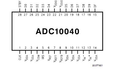
DSP Front EndsPinout Specifications
 Description
The ADC10040 is a monolithic CMOS analog-to-digital con- verter capable of converting analog input signals into 10-bit digital words at 40 Megasamples per second (MSPS). This converter uses a differential, pipeline architecture with digital error correction and an on-chip sample-and-hold circuit to provide a complete conversion solution, and to minimize power consumption, while providing excellent dynamic per- formance. A unique sample-and-hold stage yields a full-power bandwidth of 400 MHz. Operating on a single 3.0V power supply, this device consumes just 55.5 mW at
40 MSPS, including the reference current. The Standby feature reduces power consumption to just 13.5 mW.
The differential inputs of ADC10040 provide a full scale selectable input swing of 2.0 VP-P, 1.5 VP-P, 1.0 VP-P, with the possibility of a single-ended input. Full use of the differential input is recom-mended for optimum performance. An internal +1.2V preci-sion bandgap reference is used to set the ADC full-scale range, and also allows the user to supply a buffered refer-enced voltage for those applications requiring increased ac-curacy. The output data format is 10-bit offset binary, or two's complement.
This device ADC10040 is available in the 28-lead TSSOP package and will operate over the industrial temperature range of −40˚C to +85˚C.

 ADC10040 Data Sheet


