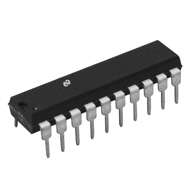
Pinout Specifications
| Resolution | 12 bits |
| Channels | 2 Channels |
| SNR | 47 dB |
| SFDR | 55.5 dB |
| ENOB | 7.4 bits |
| Max Sample Rate | 1500 MSPS |
| Min Sample Rate | 200 MSPS |
| Power Dissipation | 2 Watt |
| PowerWise Rating 1 | 3.95 pJ/conv |
| DNL (+/-) | 0.15 LSB |
| INL (+/-) | 0.3 LSB |
| SINAD | 46.3 dB |
| THD dB | -53.4 dB |
| Min Supply Voltage | 1.8 Volt |
| Max Supply Voltage | 2 Volt |
| Nominal Vin | 0.9 Vpp |
| Temperature Min | -55 deg C |
| Temperature Max | 125 deg C |
| Data Converter Type | ADC |
| AEC Q-100 Automotive Grade | 0 |
| Radiation Performance - Total Dose (TID) | 300 Krad |
| Radiation Performance - SEL (MeV) | 120 |
| View Using Catalog |
DescriptionThe ADC08D1520 is an 8Bit, dual channel, low power, high performance CMOS analog-to-digital converter that builds upon the ADC08D1000 platform. The ADC08D1520 digitizes signals to 8 bits of resolution at sample rates up to 1.7 GSPS. It has expanded features compared to the ADC08D1000, which include a test pattern output for system debug, clock phase adjust, and selectable output demultiplexer modes. Consuming a typical 2.0W in Demultiplex Mode at 1.5 GSPS from a single 1.9 Volt supply, this device is guaranteed to have no missing codes over the full operating temperature range. The unique folding and interpolating architecture, the fully differential comparator design, the innovative design of the internal sample-and-hold amplifier and the self-calibration scheme enable a very flat response of all dynamic parameters beyond Nyquist, producing a high 7.2 Effective Number of Bits (ENOB) with a 748 MHz input signal and a 1.5 GHz sample rate while providing a 10 -18 Code Error Rate (C.E.R.) Output formatting is offset binary and the Low Voltage Differential Signaling (LVDS) digital outputs are compatible with IEEE 1596.3-1996, with the exception of an adjustable common mode voltage between 0.8V and 1.2V.
Each converter ADC08D1520QML has a selectable output demultiplexer which feeds two LVDS buses. If the 1:2 Demultiplexed Mode is selected, the output data rate is reduced to half the input sample rate on each bus. When Non-Demultiplexed Mode is selected, that output data rate on channels DI and DQ are at the same rate as the input sample clock. The two converters can be interleaved and used as a single 3 GSPS ADC.
The ADC08D1520QML converter typically consumes less than 2.9 mW in the Power Down Mode and is available in a 128-pin, thermally enhanced, multi-layer ceramic quad package and operates over the Military (-55°C TA +125°C) temperature range.
Reliability Metrics
| Part Number |
Process |
EFR Reject |
EFR Sample Size |
PPM |
LTA Rejects |
LTA Device Hours |
FITS |
MTTF (Hours) |
| ADC08D1520WGFQV |
CMOS9 |
1 |
6382 |
157 |
0 |
923000 |
4 |
261903770 |
Note: The Early Failure Rates (EFR) were calculated as point estimate PPM based on rejects and sample size for EFR. The Long Term Failure Rates were calculated at 60% confidence using the Arrhenius equation at 0.7eV activation energy and derating the assumed stress temperature of 150°C to an application temperature of 55°C.For more information on Reliability Metrics, please click here.

 ADC08D1520QML Data Sheet