Architecture
: SAR
Mounting Style
: SMD/SMT
Packaging
: Tube
Input Type
: Voltage
SNR
: Yes
Number of Converters
: 1
Number of ADC Inputs
: 1
Voltage Reference
: External
Resolution
: 8 bit
Supply Voltage - Min
: 4.5 V
Interface Type
: Parallel
Maximum Operating Temperature
: + 70 C
Maximum Power Dissipation
: 875 mW
Conversion Rate
: 10 KSPs
Supply Voltage - Max
: 6.3 V
Package / Case
: SOIC-20 Wide
Pinout Description
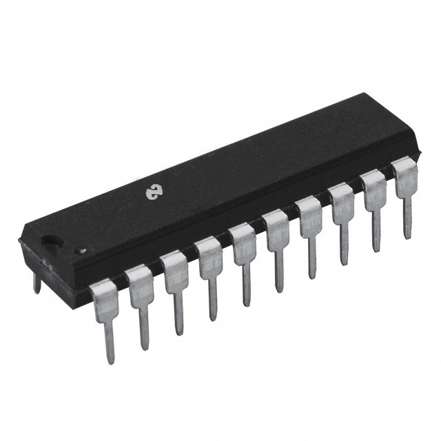
The ADC0804LCWM is one member of the ADC0804 series.The ADC0804 family are CMOS 8-Bit, successive-approximation A/D converters which use a modified potentiometric ladder and are designed to operate with the 8080A control bus via three-state outputs. These converters appear to the processor as memory locations or I/O ports, and hence no interfacing logic is required.
Features of the ADC0804LCWM are:(1)conversion time < 100s; (2) easy interface to most microprocessors; (3)will operate in a "stand alone" mode; (4) differential analog voltage inputs; (5) works with bandgap voltage references; (6) ttl compatible inputs and outputs; (7) on-chip clock generator; (8) 0v to 5v analog voltage input range (single + 5v supply); (9)no zero-adjust required.The differential analog voltage input has good common-mode-rejection and permits offsetting the analog zero-input-voltage value. In addition, the voltage reference input can be adjusted to allow encoding any smaller analog voltage span to the full 8 bits of resolution.
The absolute maximum ratings of the ADC0804LCWM can be summarized as:(1)supply voltage:6.5v;(3)voltage at any input:-0.3V to (v+ +0.3V);(3)maximum storage temperature range:-65 to 150;(4)maximum lead temperature (soldering, 10s) :300 . Stresses above those listed in "Absolute Maximum Ratings" may cause permanent damage to the device. This is a stress only rating and operation of the device at these or any other conditions above those indicated in the operational sections of this specification is not implied.The internal switching action causes displacement currents to flow at the analog inputs. The voltage on the on-chip capacitance to ground is switched through the analog differentia input voltage, resulting in proportional currents entering the VIN(+) input and leaving the VIN(-) input. These current transients occur at the leading edge of the internal clocks. They rapidly decay and do not inherently cause errors as the on chip comparator is strobed at the end of the clock perIod.

 ADC0804LCWM Data Sheet


