Packaging
:
Mounting Style
: SMD/SMT
Input Type
: Voltage
Number of Converters
: 1
Number of ADC Inputs
: 1
Voltage Reference
: External
Supply Voltage - Max
: 5.25 V
Resolution
: 8 bit
Interface Type
: Parallel
Supply Voltage - Min
: 4.75 V
Architecture
: Flash
Maximum Operating Temperature
: + 75 C
SNR
: 46 dB
Conversion Rate
: 100 MHz
Package / Case
: QFP-48
Maximum Power Dissipation
: 960 mW
Features: • Low power dissipation (960mW max.)
• TTL compatible output
• Diff./Integral nonlinearity (±½LSB max.)
• 1:2 Demultiplexed straight output programmable
• 2:1 Frequency divided TTL clock output with reset
• Surface mount package
• Selectable Input Logic (TTl, ECL, PECL)
• +5V or ±5V Power Supply OperationPinout SpecificationsSupply Voltage (+AVS, +DVS, 1,2) 0.5 to +7.0 Volts
Supply Voltage (AGND, DGND 1, 2) 0.5 to +7.0 Volts
Supply Voltage (DGND 3) 0.5 to +7.0 Volts
Supply Voltage (DVS) À 0.5 to +7.0 Volts
Supply Voltage (DVS) Á 7.0 to +0.5 Volts
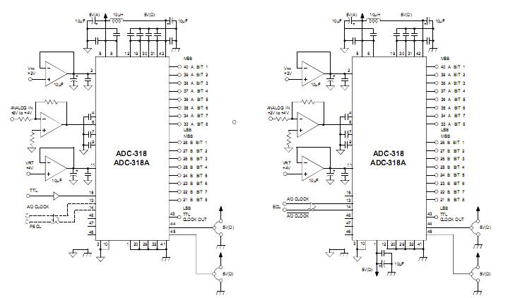
Reference Voltage (VRT) +2.7 to +AVS VoltsDescriptionThe ADC-318 and ADC-318A are 8 bit monolithic bipolar, full flash A/D converters. Though they have high, 120MHz (ADC-318) and 140MHz (ADC-318A), sampling rates, their input logic level, including the start convert pulse, is TTL, ECL and PECL compatible. Digital outputs are also TTL compatible and allow a straight output or a programmable 1:2 de-multiplexed output.
The ADC-318 and ADC-318A feature ±1/2 LSB max. integral and differential non-linearity, +5V single or ±5V dual power supply operation, a low 960mW maximum power dissipation, 150MHz wide analog input range and excellent temperature coefficient in a small 48 pin QFP package. The start convert pulse can have a 50% duty cycle. The ADC-318 and ADC-318A offer low cost, easy to use functionality for design engineers.

 ADC-318A Data Sheet


