AD9246

Features: 1.8 V analog supply operation1.8 V to 3.3 V output supplySNR = 71.7 dBc (72.7 dBFS) to 70 MHz inputSFDR = 85 dBc to 70 MHz inputLow power: 395 mW @ 125 MSPSDifferential input with 650 MHz bandwidthOn-chip voltage reference and sample-and-hold amplifierDNL = ±0.4 LSBFlexible analog input:...

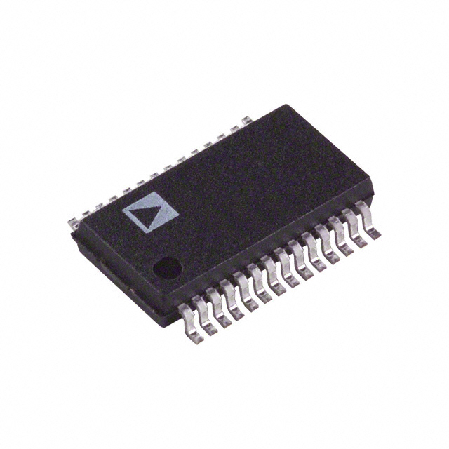
product image

AD9246 Picture
SeekIC No. : 004272989 Detail

AD9246: Features: 1.8 V analog supply operation1.8 V to 3.3 V output supplySNR = 71.7 dBc (72.7 dBFS) to 70 MHz inputSFDR = 85 dBc to 70 MHz inputLow power: 395 mW @ 125 MSPSDifferential input with 650 MHz ...

floor Price/Ceiling Price

Part Number:
AD9246
Supply Ability:
5000

Price Break

  • Qty
  • 1~5000
  • Unit Price
  • Negotiable
  • Processing time
  • 15 Days
Total Cost: $ 0.00

SeekIC Buyer Protection PLUS - newly updated for 2013!

  • Escrow Protection.
  • Guaranteed refunds.
  • Secure payments.
  • Learn more >>

Month Sales

268 Transactions

Rating

evaluate  (4.8 stars)

Upload time: 2024/11/24

Payment Methods

All payment methods are secure and covered by SeekIC Buyer Protection PLUS.

Notice: When you place an order, your payment is made to SeekIC and not to your seller. SeekIC only pays the seller after confirming you have received your order. We will also never share your payment details with your seller.
Product Details

Description


Features:

1.8 V analog supply operation
1.8 V to 3.3 V output supply
SNR = 71.7 dBc (72.7 dBFS) to 70 MHz input
SFDR = 85 dBc to 70 MHz input
Low power: 395 mW @ 125 MSPS
Differential input with 650 MHz bandwidth
On-chip voltage reference and sample-and-hold amplifier
DNL = ±0.4 LSB
Flexible analog input: 1 V p-p to 2 V p-p range
Offset binary, Gray code, or twos complement data format
Clock duty cycle stabilizer
Data output clock
Serial port control
Built-in selectable digital test pattern generation
Programmable clock and data alignment


Application

IF sampling in communications receivers
IS-95, CDMA-One, IMT-2000
Battery-powered instruments
Hand-held scopemeters
Low cost digital oscilloscopes


Pinout

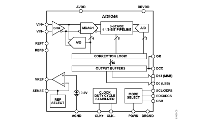
AD9246 Diagram


Specifications

Parameter Rating
ELECTRICAL AVDD to AGND
DRVDD to DRGND
AGND to DRGND
AVDD to DRVDD
D0 through D11 to DRGND
DCO to DRGND
OR to DRGND
CLK+ to AGND
CLK− to AGND
VIN+ to AGND
VIN− to AGND
VREF to AGND
SENSE to AGND
REFT to AGND
REFB to AGND
SDIO/DCS to DRGND
PDWN to AGND
CSB to AGND
SCLK/DFS to AGND
OEB to AGND

−0.3 V to +2.0 V
−0.3 V to +3.9 V
−0.3 V to +0.3 V
−3.9 V to +2.0 V
−0.3 V to DRVDD + 0.3 V
−0.3 V to +3.9 V
−0.3 V to +3.9 V
−0.3 V to AVDD + 1.3 V
−0.3 V to AVDD + 0.2 V
−0.3 V to DRVDD + 0.3 V
−0.3 V to +3.9 V
−0.3 V to +3.9 V
−0.3 V to +3.9 V
−0.3 V to +3.9 V

ENVIRONMENTAL
Storage Temperature Range
Operating Temperature Range
Lead Temperature (Soldering 10 Sec)
Junction Temperature


65°C to +125°C
40°C to +85°C
300°C
150°C


Resolution (Bits) 14bit
T-Put Rate 125MSPS
# Chan 1
Supply V Multi(+1.8Anlg, +1.8Dig)
Pwr Diss 458mW
Interface Par
Ain Range (2Vref) p-p,1 V p-p,2 V p-p
SNR (dB) 71.9dB
Pkg Type CSP


Description

The AD9246 is a monolithic, single 1.8 V supply, 14-bit, 80 MSPS/ 105 MSPS/125 MSPS analog-to-digital converter (ADC), featuring a high performance sample-and-hold amplifier (SHA) and on-chip voltage reference. The product uses a multistage differential pipeline architecture with output error correction logic to provide 14-bit accuracy at 125 MSPS data rates and guarantees no missing codes over the full operating temperature range.

The wide bandwidth, truly differential SHA allows a variety of user-selectable input ranges and offsets, including single-ended applications. It is suitable for multiplexed systems that switch full-scale voltage levels in successive channels and for sampling single-channel inputs at frequencies well beyond the Nyquist rate. Combined with power and cost savings over previously available ADCs, the AD9246 is suitable for applications in communications, imaging, and medical ultrasound.

A differential clock input controls all internal conversion cycles. A duty cycle stabilizer (DCS) compensates for wide variations in the clock duty cycle while maintaining excellent overall ADC performance

The digital output data is presented in offset binary, Gray code, or twos complement formats. A data output clock (DCO) is provided to ensure proper latch timing with receiving logic.

The AD9246 is available in a 48-lead LFCSP_VQ and is specified over the industrial temperature range (−40°C to +85°C).


Customers Who Bought This Item Also Bought

Margin,quality,low-cost products with low minimum orders. Secure your online payments with SeekIC Buyer Protection.
Inductors, Coils, Chokes
Fans, Thermal Management
Batteries, Chargers, Holders
Crystals and Oscillators
Power Supplies - Board Mount
Transformers
View more