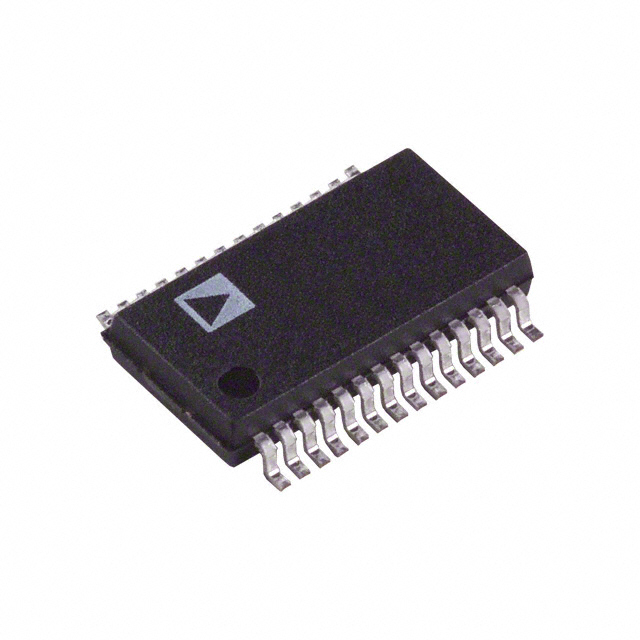
Features: Monolithic 12-Bit A/D Converter Product Family
Family Members Are: AD9221, AD9223, and AD9220
Flexible Sampling Rates: 1.5 MSPS, 3.0 MSPS and 10.0 MSPS
Low Power Dissipation: 59 mW, 100 mW and 250 mW
Single +5 V Supply
Integral Nonlinearity Error: 0.5 LSB
Differential Nonlinearity Error: 0.3 LSB
Input Referred Noise: 0.09 LSB
Complete: On-Chip Sample-and-Hold Amplifier and Voltage Reference
Signal-to-Noise and Distortion Ratio: 70 dB
Spurious-Free Dynamic Range: 86 dB
Out-of-Range Indicator
Straight Binary Output Data
28-Lead SOIC and 28-Lead SSOPPinout Specifications
| Parameter |
With Respect to |
Min |
Max |
Units |
| AVDD |
AVSS |
0.3 |
+6.5 |
V |
| DRVDD |
DRVSS |
0.3 |
+6.5 |
V |
| AVSS |
DRVSS |
0.3 |
+0.3 |
V |
| AVDD |
DRVDD |
6.5 |
+6.5 |
V |
| MODE |
AVSS |
0.3 |
AVDD + 0.3 |
V |
| CLK |
AVSS |
0.3 |
AVDD + 0.3 |
V |
| Digital Outputs |
DRVSS |
0.3 |
DRVDD + 0.3 |
V |
| AIN |
AVSS |
0.3 |
AVDD + 0.3 |
V |
| VREF |
AVSS |
0.3 |
AVDD + 0.3 |
V |
| REFSENSE |
AVSS |
0.3 |
AVDD + 0.3 |
V |
| REFTF, REFTB |
AVSS |
0.3 |
AVDD + 0.3 |
V |
| REFTS, REFBS |
AVSS |
0.3 |
AVDD + 0.3 |
V |
| Junction Temperature |
|
|
+150 |
°C |
| Storage Temperature |
|
65 |
+150 |
°C |
Lead Temperature
10 sec |
|
|
+300 |
°C |
| Resolution (Bits) |
12bit |
| T-Put Rate |
10MSPS |
| # Chan |
1 |
| Supply V |
Single(+5) |
| Pwr Diss |
310mW |
| Interface |
Par |
| Ain Range |
2 V p-p,5V p-p |
| SNR (dB) |
70.2dB |
| Pkg Type |
SOIC,SOP |
DescriptionThe AD9221, AD9223, and AD9220 are a generation of high performance, single supply 12-bit analog-to-digital converters. Each device exhibits true 12-bit linearity and temperature drift performance1 as well as 11.5 bit or better ac performance.2 The AD9221/AD9223/AD9220 share the same interface options, package, and pinout. Thus, the product family provides an upward or downward component selection path based on performance, sample rate and power. The devices differ with respect to their specified sampling rate and power consumption which is reflected in their dynamic performance over frequency.
The AD9221/AD9223/AD9220 combine a low cost, high speed CMOS process and a novel architecture to achieve the resolution and speed of existing hybrid and monolithic implementations at a fraction of the power consumption and cost. Each device is a complete, monolithic ADC with an on-chip, high performance, low noise sample-and-hold amplifier and programmable voltage reference. An external reference can also be chosen to suit the dc accuracy and temperature drift requirements of the application.The devices use a multistage differential pipelined architecture with digital output error correction logic to provide 12-bit accuracy at the specified data rates and to guarantee no missing codes over the full operating temperature range.
The input of the AD9221/AD9223/AD9220 is highly flexible, allowing for easy interfacing to imaging, communications, medical, and data-acquisition systems. A truly differential input structure allows for both single-ended and differential input interfaces of varying input spans. The sample-and-hold (SHA) amplifier is equally suited for both multiplexed systems that switch full-scale voltage levels in successive channels as well as sampling single-channel inputs at frequencies up to and beyond the Nyquist rate. Also, the AD9221/AD9223/AD9220 is well suited for communication systems employing Direct-IF Down Conversion since the SHA in the differential input mode can achieve excellent dynamic performance far beyond its specified Nyquist frequency.
2
A single clock input is used to control all internal conversion cycles. The digital output data is presented in straight binary output format. An out-of-range (OTR) signal indicates an overflow condition which can be used with the most significant bit to determine low or high overflow.

 AD9220 Data Sheet


