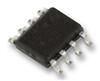
Specifications
| Logic Output |
LVDS |
| # Per Pkg |
1 |
| Prop Delay (ns)typ |
1.5ns |
| Voltage Supply (V) |
2.5 to 5.5 |
| Min Pulse Width |
1ns |
| Package |
12-Lead LFCSP |
| Latch Enable Pin |
X |
DescriptionThe AD8465 is a very fast comparator fabricated on the Analog Devices, Inc., proprietary XFCB2 process. Split input/output supplies, with no sequencing restrictions, support a wide input signal range with greatly reduced power consumption. This comparator is exceptionally versatile and easy to use. A flexible power supply scheme allows the devices to operate with a single 2.5 V positive supply and a -0.5 V to +2.7 V input signal range up to a 5.5 V positive supply with a -0.5 V to +5.7 V input signal range. The LVDS-compatible output stage is designed to drive any standard LVDS input. The comparator input stage offers robust protection against large input overdrive, and the outputs do not phase reverse when the valid input signal range is exceeded. High speed latch and programmable hysteresis features are also provided in a unique single-pin control option. The AD8465 is available in a 12-lead LFCSP. Features include an input range from VEE 0.5 V to VCCI + 0.2 V, low noise, LVDS- compatible output drivers, and TTL/CMOS latch inputs with adjustable hysteresis and/or shutdown inputs. The device offers 1.6 ns propagation delay with 1 ps rms random jitter (RJ). Overdrive and slew rate dispersion are typically less than 50 ps.
The features of AD8465 can be summarized as (1)fully specified rail to rail at VCCI = 2.5 V to 5.5 V; (2)input common-mode voltage from -0.2 V to VCCI + 0.2 V; (3)low glitch LVDS-compatible output stage; (4)propagation delay: 1.6 ns; (5)power dissipation: 37 mW at 2.5 V; (6)shutdown pin; (7)single-pin control for programmable hysteresis and latch; (8)power supply rejection > 60 dB; (9)-40°C to +125°C operation.
The absolute maximum ratings of AD8465 are (1)supply voltages input supply voltage (VCCI to GND): -0.5 V to +6.0 V/ output supply voltage (VCCO to GND): -0.5 V to +6.0 V/ positive supply differential (VCCI - VCCO): -6.0 V to +6.0 V; (2)input voltages input voltage: -0.5 V to VCCI + 0.5 V/ differential input voltage: ±(VCCI + 0.5 V)/; (3)maximum input/output current: ±50 mA; (4)shutdown control pin applied voltage (SDN to GND): -0.5 V to VCCO + 0.5 V/ maximum input/output current: ±50 mA; (5)latch/hysteresis control pin applied voltage (LE/HYS to GND)-0.5 V to VCCO + 0.5 V/ maximum input/output current: ±50 mA; (6)output current: ±50 mA; (7)temperature: operating temperature range, ambient: -40°C to +125°C/ operating temperature, junction: 150°C/ storage temperature range: -65°C to +150°C.

 AD8465 Data Sheet