AD8382

Features: High accuracy, high resolution voltage outputs12-bit input resolutionLaser trimmed outputs Fast settling, high voltage drive33 ns settling time to 0.25% into 200 pF loadSlew rate 390 V/µsOutputs to within 1.3 V of supply High update ratesFast, 120 Ms/s data update rate Voltage con...

product image

AD8382 Picture
SeekIC No. : 004272261 Detail

AD8382: Features: High accuracy, high resolution voltage outputs12-bit input resolutionLaser trimmed outputs Fast settling, high voltage drive33 ns settling time to 0.25% into 200 pF loadSlew rate 390 V/&m...

floor Price/Ceiling Price

Part Number:
AD8382
Supply Ability:
5000

Price Break

  • Qty
  • 1~5000
  • Unit Price
  • Negotiable
  • Processing time
  • 15 Days
Total Cost: $ 0.00

SeekIC Buyer Protection PLUS - newly updated for 2013!

  • Escrow Protection.
  • Guaranteed refunds.
  • Secure payments.
  • Learn more >>

Month Sales

268 Transactions

Rating

evaluate  (4.8 stars)

Upload time: 2024/12/21

Payment Methods

All payment methods are secure and covered by SeekIC Buyer Protection PLUS.

Notice: When you place an order, your payment is made to SeekIC and not to your seller. SeekIC only pays the seller after confirming you have received your order. We will also never share your payment details with your seller.
Product Details

Description


Features:

High accuracy, high resolution voltage outputs
12-bit input resolution
Laser trimmed outputs
Fast settling, high voltage drive
33 ns settling time to 0.25% into 200 pF load
Slew rate 390 V/µs
Outputs to within 1.3 V of supply
High update rates
Fast, 120 Ms/s data update rate
Voltage controlled video reference (brightness) and
full-scale (contrast) output levels
Flexible logic
STSQ/XFR allow parallel AD8382 operation
INV bit reverses polarity of video signal
Output overload protection
Low static power dissipation: 743 mW
Includes STBY function
3.3 V logic, 9 V to 18 V analog supplies
Available in 48-lead 7 mm * 7 mm LFCSP


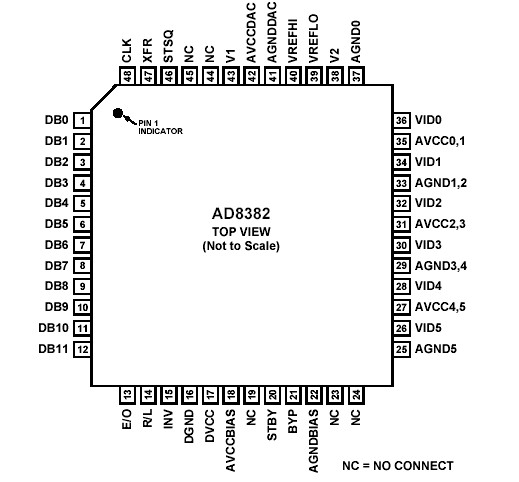
Pinout

  Connection Diagram

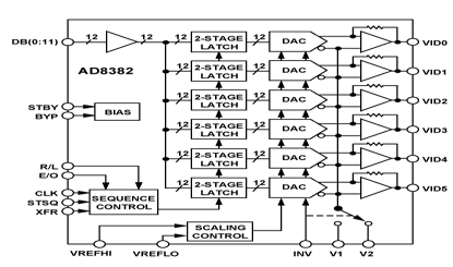
AD8382 Diagram


Specifications

Parameter Rating
Supply Voltages
AVCCx AGNDx
DVCC DGND
Input Voltages
Maximum Digital Input Voltage
Minimum Digital Input Voltage
Maximum Analog Input Voltage
Minimum Analog Input Voltages
Internal Power Dissipation2
TQFP E-Pad Package @ 25°C Ambient
Operating Temperature Range
Storage Temperature Range
Lead Temperature Range (Soldering 10 sec)

18 V
4.5 V

DVCC + 0.5 V
DGND 0.5 V
AVCC + 0.5 V
AGND 0.5 V

3.84 W
0°C to 85°C
65°C to +125°C
300°C


Description

The AD8382 DecDriver provides a fast, 12-bit latched decimat-ing digital input that drives six high voltage outputs.12-bit input words are sequentially loaded into six separate, high speed, bipolar DACs. A flexible digital input format allows several AD8382s to be used in parallel for higher resolution displays.

STSQ synchronizes sequential input loading, XFR controls synchronous output updating, and R/L controls the direction of loading as either left-to-right or right-to-left. Six channels of high voltage output drivers drive to within 1.3 V of the rail. The output signal can be adjusted for dc reference, signal inversion, and contrast for maximum flexibility.

The AD8382 is fabricated on Analog Devices' XFHV, fast bipolar 26 V process, providing fast input logic bipolar DACs with trimmed accuracy and fast settling, high voltage, precision drive amplifiers on the same chip. The AD8382 dissipates 743 mW nominal static power. The STBY pin reduces power to a minimum, with fast recovery.


Customers Who Bought This Item Also Bought

Margin,quality,low-cost products with low minimum orders. Secure your online payments with SeekIC Buyer Protection.
Hardware, Fasteners, Accessories
Power Supplies - Board Mount
Static Control, ESD, Clean Room Products
Motors, Solenoids, Driver Boards/Modules
Fans, Thermal Management
Integrated Circuits (ICs)
View more