Features: High Voltage Drive:
Rated Settling Time to within 1.3 V of Supply Rails
Output Overload Protection
High Update Rates:
Fast, 100 Ms/s 10-Bit Input Word Rate
Low Power Dissipation: 570 mW
Includes STBY Function
Voltage Controlled Video Reference (Brightness) and
Full-Scale (Contrast) Output Levels
3.3 V or 5 V Logic and 9 V18 V Analog Supplies
High Accuracy:
Laser Trimming Eliminates External Calibration
Flexible Logic:
INV Reverses Polarity of Video Signal
STSQ/XFR for Parallel AD8381 Operation in
12-Channel Systems
Drives Capacitive Loads:
27 ns Settling Time to 1% into 150 pF Load
Slew Rate 265 V/s with 150 pF Load
Available in 48-Lead LQFP
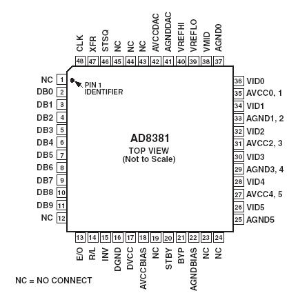
ApplicationLCD Analog Column DriverPinout
 SpecificationsSupply Voltages
AVCCx AGND . . . . . . . . . . . . . . . . . . . .. .. ... . . . . . . . . . . 19 V
DVCC DGND . . . . . . . . . . . . . . . . . . . . .. .. .. .. . . . . . . . . . . 5.5 V
Input Voltages
Maximum Digital Input Voltages . . . . . . . .. .. .. ... . DVCC + 0.5 V
Minimum Digital Input Voltages . . . . . .. .. .. .. .. . . DGND 0.5 V
Maximum Analog Input Voltages . . . . . . . . . . .. .. . AVCC + 0.5 V
Minimum Analog Input Voltages . . . . . .. . . . . . . . AGND 0.5 V
Internal Power Dissipation2
LQFP Package @ 25°C Ambient . . . . . . . . .. . . . . . . . . . . 2.7 W
Output Short Circuit Duration . . . . . . . . . . . . . . . . . .. . . . . . Infinite
Operating Temperature Range . . . . . . . . . . ... . . . . . 0°C to 85°C
Storage Temperature Range . . . . . . . . . .. . . . 65°C to +125°C
Lead Temperature Range (Soldering 10 sec) . . . . . . . .. . . . 300°C
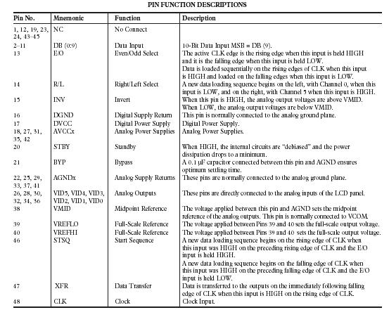
DescriptionThe AD8381 provides a fast, 10-bit latched decimating digital input, which drives six high voltage outputs. Ten-bit input words are sequentially loaded into six separate high-speed, bipolar DACs. Flexible digital input format allows several AD8381s to be used in parallel for higher resolution displays. STSQ synchronizes sequential input loading, XFR controls synchronous output updating and R/L controls the direction of loading as either Left to Right or Right to Left. Six channels of high voltage output drivers drive to within 1.3 V of the rail in rated settlingtime. The output signal can be adjusted for brightness, signal inversion and contrast for maximum flexibility.
The AD8381 is fabricated on ADI's proprietary, fast bipolar 24 V process, providing fast input logic, bipolar DACs with trimmed accuracy and fast settling, high voltage precision drive amplifiers on the same chip.
The AD8381 dissipates 570 mW nominal static power. STBY pin reduces power to a minimum, with fast recovery.
The AD8381 is offered in a 48-lead 7 * 7 * 1.4 mm LQFP package and operates over the commercial temperature range of 0°C to 85°C.

 AD8381 Data Sheet


