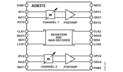
Features: `Dual independent digitally controlled VGA
`Differential input and output
150 differential input
Open-collector differential output
`7.8 dB noise figure to 100 MHz @ maximum gain
`HD2/HD3 better than 77 dBc for 1 V p-p differential output
`3 dB bandwidth of 150 MHz
`41 dB gain range
`1 dB step size ±0.2 dB
`Serial 8-bit bidirectional SPI control interface
`Wide input dynamic range
`Pin-programmable output stage
`Power-down feature
`Single 5 V supply: 106 mA per channel
`32-lead LFCSP, 5 mm*5 mm packageApplication·Differential ADC drivers
·CMTS upstream direct sampling receivers
·CATV modem signal scaling
·Generic RF/IF gain stages
·Single-ended-to-differential conversion Pinout
 Specifications
| Supply Voltage (V) |
+5V |
| Gain Low End (dB) |
-9dB |
| Gain High End (dB) |
+32dB |
| -3 dB BW (MHz) |
130MHz |
| Gain Accuracy (dB) |
±0.3dB |
| Supply Current |
116mA |
| Package |
32-Lead CSP |
DescriptionThe AD8372 is a dual, digitally controlled, variable gain amplifier that provides precise gain control, high IP3, and low noise figure. The excellent distortion performance and moderate signal
The AD8372 is a dual, digitally controlled, variable gain amplifier that provides precise gain control, high IP3, and low noise figure. The excellent distortion performance and moderate signal bandwidth make the AD8372 a suitable gain control device for a variety of multichannel receiver
applications.
For wide input dynamic range applications, the AD8372 provides a broad 41 dB gain range. The gain is programmed through a bidirectional 4-pin serial interface. The serial inter-face consists of a clock, latch, data input, and data output lines for each channel.
The AD8372 provides the ability to set the transconductance of the output stage using a single external resistor. The RXT1 and RXT2 pins provide a band gap derived stable reference voltage of 1.56 V. Typically 2.0 k shunt resistors to ground are used to set the maximum gain to a nominal value of 31 dB. The current setting resistors can be adjusted to manipulate the gain and distortion performance of each channel. This is a flexible feature in applications where it is desirable to trade off distortion performance for lower power consumption.
The AD8372 is powered on by applying the appropriate logic level to the ENB1, ENB2 pins. When powered down, the AD8372 consumes less than 2.6 mA and offers excellent input-to-output isolation. The gain setting is preserved when powered down.
Fabricated on an Analog Devices high frequency BiCMOS process, the AD8372 provides precise gain adjustment capabilities with good distortion performance. The quiescent current of the AD8372 is typically 106 mA per channel. The AD8372 amplifier comes in a compact, thermally enhanced 5 mm 5 mm 32-leadLFCSP package and operates over the temperature range of 40 to +85

 AD8372 Data Sheet


