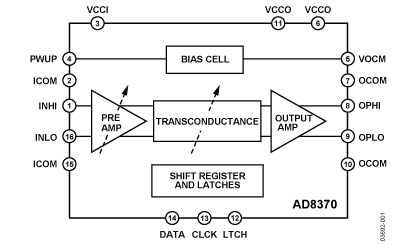
Features: Programmable low and high gain (<2 dB resolution)
Low range: −11 dB to +17 dB
High range: +6 dB to +34 dB
Differential input and output:
200 differential input
100 differential output
7 dB noise figure @ maximum gain
Two-tone IP3 of +35 dBm @ 70 MHz
−3 dB bandwidth of 750 MHz
40 dB precision gain range
Serial 8-bit digital interface
Wide input dynamic range
Power-down feature
Single 3 V to 5 V supply
ApplicationDifferential ADC drivers
IF sampling receivers
RF/IF gain stages
Cable and video applications
SAW filter interfacing
Single-ended-to-differential conversionPinout

| Pin No. |
Mnemonic |
Description |
| 1 |
INHI |
Balanced Differential Input. Internally biased. |
| 2,15 |
ICOM |
Input Common. Connect to a low impedance ground. This node is also connected to the exposed pad on the bottom of the device. |
| 3 |
VCCI |
Input Positive Supply. 3.0 V to 5.5 V. Should be properly bypassed. |
| 4 |
PWUP |
Power Enable Pin. Device is operational when PWUP is pulled high. |
| 5 |
VOCM |
Common-Mode Output Voltage Pin. The midsupply ((VVCCO − VOCOM)/2) common-mode voltage is delivered to this pin for external bypassing for additional common-mode supply decoupling. This can be achieved with a bypass capacitor to ground. This pin is an output only and is not to be driven externally. |
| 6,11 |
VCCO |
Output Positive Supply. 3.0 V to 5.5 V. Should be properly bypassed. |
| 7,10 |
OCOM |
Output Common. Connect to a low impedance ground. |
| 8 |
OPHI |
Balanced Differential Output. Biased to midsupply. |
| 9 |
OPLO |
Balanced Differential Output. Biased to midsupply. |
| 12 |
LTCH |
Serial Data Latch Pin. Serial data is clocked into the shift register via the DATA pin when LTCH is low. Data in shift register is latched on the next high-going edge. |
| 13 |
CLCK |
Serial Clock Input Pin. |
| 14 |
DATA |
Serial Data Input Pin. |
| 15 |
INLO |
Balanced Differential Input. Internally biased. |
Specifications
| Gain Control |
Digital |
| -3 dB BW (MHz) |
700MHz |
| Gain Low End (dB) |
+25dB |
| Gain High End (dB) |
+34dB |
| Number of Channels |
1 |
| Spectral Noise (nV/rtHz) |
2.1nV/rtHz |
| Supply Voltage (V) |
+5.5V |
| Supply Current |
78mA |
| Parameter |
Rating |
| Supply Voltage, VS |
5.5 V |
| PWUP, DATA, CLCK, LTCH |
VS + 500 mV |
|
Differential Input Voltage,
VINHI VINLO |
2 V |
|
Common-Mode Input Voltage, VINHI or
VINLO, with respect to ICOM or OCOM |
VS + 500 mV
(maximum),
VICOM 500 mV,
VOCOM 500 mV
(minimum) |
| Internal Power Dissipation |
575 mW |
| JA (Exposed paddle soldered down) |
30°C/W |
| JA (Exposed paddle not soldered down) |
95°C/W |
| JC (At exposed paddle) |
9°C/W |
| Maximum Junction Temperature |
150°C |
| Operating Temperature Range |
40°C to +85°C |
| Storage Temperature Range |
65°C to +150°C |
|
Lead Temperature Range
(Soldering 60 sec) |
235°C |
Stresses above those listed under Absolute Maximum Ratings may cause permanent damage to the device. This is a stress rating only; functional operation of the device at these or any other conditions above those listed in the operational sections of this specification is not implied. Exposure to absolute maximum rating conditions for extended periods may affect device reliability.DescriptionThe AD8370 is a low cost, digitally controlled, variable gain amplifier that provides precision gain control, high IP3, and low noise figure. The excellent distortion performance and wide bandwidth make the AD8370 a suitable gain control device for modern receiver designs.
For wide input, dynamic range applications, the AD8370 pro-vides two input ranges: high gain mode and low gain mode. A vernier 7-bit transconductance (Gm) stage provides 28 dB of gain range at better than 2 dB resolution, and 22 dB of gain range at better than 1 dB resolution. A second gain range, 17 dB higher than the first, can be selected to provide improved noise performance.
The AD8370 is powered on by applying the appropriate logic level to the PWUP pin. When powered down, the AD8370 consumes less than 4 mA and offers excellent input to output isolation. The gain setting is preserved when operating in a power-down mode.
Gain control of the AD8370 is through a serial 8-bit gain control word. The MSB selects between the two gain ranges, and the remaining 7 bits adjust the overall gain in precise linear gain steps.
Fabricated on the ADI high speed XFCB process, the high band-width of the AD8370 provides high frequency and low distortion. The quiescent current of the AD8370 is 78 mA typically. The AD8370 amplifier comes in a compact, thermally enhanced 16-lead TSSOP package and operates over the temperature range of −40°C to +85°C.

 AD8370 Data Sheet


