Features: `Calibrated RMS Response`Excellent Temperature Stability`Up to 30 dB Input Range at 2.5 GHz`700 mV rms, 10 dBm re 50 Maximum Input`±0.25 dB Linear Response Up to 2.5 GHz`Single Supply Operation: 2.7 V to 5.5 V`Low Power: 3.3 mW at 3 V Supply`Rapid Power-Down to Less than 1 AApplication·...
AD8361: Features: `Calibrated RMS Response`Excellent Temperature Stability`Up to 30 dB Input Range at 2.5 GHz`700 mV rms, 10 dBm re 50 Maximum Input`±0.25 dB Linear Response Up to 2.5 GHz`Single Supply Ope...
SeekIC Buyer Protection PLUS - newly updated for 2013!
268 Transactions
All payment methods are secure and covered by SeekIC Buyer Protection PLUS.
Supply Voltage VS | 5.5 V |
SREF, PWDN | 0 V, VS |
IREF | VS 0.3 V, VS |
RFIN | 1 V rms |
Equivalent Power re 50 | 13 dBm |
Internal Power Dissipation2 | 200 mW |
SOT-23-6L | 170 mW |
micro_SOIC | 200 mW |
Maximum Junction Temperature | 125 |
Operating Temperature Range | 40 to +85 |
Storage Temperature Range | -65 to +150 |
Lead Temperature Range (Soldering, 60 sec) | +300 |
NOTES
1 Stresses above those listed under Absolute Maximum Ratings may cause permanent damage to the device. This is a stress rating only; functional operation of the device at these or any other conditions above those indicated in the operational section of this specification is not implied. Exposure to absolute maximum rating conditions for extended periods may affect device reliability.
2 Specification is for the device in free air.
SOT-23-6L: JA = 230/W; JC = 92/W.
micro_SOIC: JA = 200/W; JC = 44/W.
Voltage Supply (V) | 2.7 to 5.5 |
Supply Current | 1.1mA |
RF Freq (MHz) | 2500MHz |
Dynamic Range (dB) | 30dB |
Temp Stability (dB) | ±0.25dB |
Output Response | Linear in Voltage |
Response Time (ns) | 5000ns |
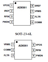
Package | 6-Lead SOT-23,8-Lead uSOIC |
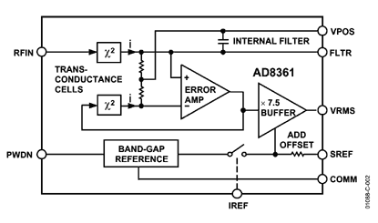
The AD8361 is a mean-responding power detector for use in highfrequency receiver and transmitter signal chains, up to 2.5 GHz. It is very easy to apply. It requires only a single supply between 2.7 V and 5.5 V, power supply decoupling capacitor and an input coupling capacitor in most applications. The output is a linear-responding dc voltage with a conversion gain of 7.5 V/V rms. An external filter capacitor can be added to increase the averaging time constant.
The AD8361 is intended for true power measurement of simple and complex waveforms. The device is particularly useful for measuring high crest-factor (high peak-to-rms ratio) signals, such as CDMA and W-CDMA.
The AD8361 has three operating modes to accommodate a variety of analog-to-digital converter requirements:
1. Ground referenced mode, in which the origin is zero;
2. Internal reference mode, which offsets the output 350 mV above ground;
3. Supply reference mode, which offsets the output to VS/7.5.
The AD8361 is specified for operation from 40 to +85 and is available in 8-lead micro_SOIC and 6-lead SOT packages. It is fabricated on a proprietary high fT silicon bipolar process.