AD7847

Features: · Two 12-Bit MDACs with Output Amplifiers· 4-Quadrant Multiplication· Space-Saving 0.3 , 24-Lead DIP and 24-Terminal SOIC Package· Parallel Loading Structure: AD7847· (8 + 4) Loading Structure: AD7837Application· Automatic Test Equipment· Function Generation· Waveform Reconstruction·Prog...

product image

AD7847 Picture
SeekIC No. : 004271023 Detail

AD7847: Features: · Two 12-Bit MDACs with Output Amplifiers· 4-Quadrant Multiplication· Space-Saving 0.3 , 24-Lead DIP and 24-Terminal SOIC Package· Parallel Loading Structure: AD7847· (8 + 4) Loading Struc...

floor Price/Ceiling Price

Part Number:
AD7847
Supply Ability:
5000

Price Break

  • Qty
  • 1~5000
  • Unit Price
  • Negotiable
  • Processing time
  • 15 Days
Total Cost: $ 0.00

SeekIC Buyer Protection PLUS - newly updated for 2013!

  • Escrow Protection.
  • Guaranteed refunds.
  • Secure payments.
  • Learn more >>

Month Sales

268 Transactions

Rating

evaluate  (4.8 stars)

Upload time: 2024/11/21

Payment Methods

All payment methods are secure and covered by SeekIC Buyer Protection PLUS.

Notice: When you place an order, your payment is made to SeekIC and not to your seller. SeekIC only pays the seller after confirming you have received your order. We will also never share your payment details with your seller.
Product Details

Description


Features:

· Two 12-Bit MDACs with Output Amplifiers
· 4-Quadrant Multiplication
· Space-Saving 0.3", 24-Lead DIP and 24-Terminal SOIC Package
· Parallel Loading Structure: AD7847
· (8 + 4) Loading Structure: AD7837


Application

· Automatic Test Equipment
· Function Generation
· Waveform Reconstruction
· Programmable Power Supplies
· Synchro Applications


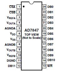
Pinout

  Connection Diagram


Specifications

VDD to DGND, AGNDA, AGNDB . . . . . ..............  0.3 V to +17 V
VSS1 to DGND, AGNDA, AGNDB . . . . . . . ...........+0.3 V to 17 V
VREFA, VREFB to AGNDA, AGNDB
. . . . . . . . . . . . . . . . . . . . . . . . . ..... VSS 0.3 V to VDD + 0.3 V
AGNDA, AGNDB to DGND . . . . . . . ...........0.3 V to VDD + 0.3 V
VOUTA2, VOUTB2 to AGNDA, AGNDB
. . . . . . . . . . . . . . . . . . . . . . . . . ..... VSS 0.3 V to VDD + 0.3 V
RFBA3, RFBB3 to AGNDA, AGNDB
. . . . . . . . . . . . . . . . . . . . . . . . . ..... VSS 0.3 V to VDD + 0.3 V
Digital Inputs to DGND . . . . . . . . . . ...... 0.3 V to VDD + 0.3 V
Operating Temperature Range
Commercial/Industrial (A, B Versions) . . ..... .40°C to +85°C
Extended (S Version) . . . . . . . . . . . . . . . ... 55°C to +125°C
Storage Temperature Range . . . . . . . . . . .  65°C to +150°C
Lead Temperature (Soldering, 10 secs) . . . . . . . . . . . . 300°C
Power Dissipation (Any Package) to +75°C . . . . . . 1000 mW
Derates above +75°C by . . . . . . . . . . . . . . . . . . . . 10 mW/°C

NOTES
1If VSS is open circuited with VDD and either AGND applied, the VSS pin will float positive, exceeding the Absolute Maximum Ratings. If this possibility exists, a Schottky diode connected between VSS and AGND (cathode to AGND) ensures the Maximum Ratings will be observed.
2The outputs may be shorted to voltages in this range provided the power dissipation of the package is not exceeded.
3AD7837 only.
*Stresses above those listed under Absolute Maximum Ratings may cause permanent damage to the device. This is a stress rating only; functional operation of the device at these or any other conditions above those listed in the operational sections of this specification is not implied. Exposure to absolute maximum rating conditions for extended periods may affect device reliability. Only one Absolute Maximum Rating may be applied at any one time.


Description

The AD7837/AD7847 is a complete, dual, 12-bit multiplying digital-to-analog converter with output amplifiers on a monolithic CMOS chip. No external user trims are required to achieve full specified performance.

Both parts are microprocessor compatible, with high speed data latches and interface logic. The AD7847 accepts 12-bit parallel data which is loaded into the respective DAC latch using the WR input and a separate Chip Select input for each DAC. The AD7837 has a double-buffered 8-bit bus interface structure with data loaded to the respective input latch in two write operations. An asynchronousLDAC signal on the AD7837 updates the DAC latches and analog outputs.

The output amplifiers are capable of developing ±10 V across a 2 k load. They are internally compensated with low input offset voltage due to laser trimming at wafer level.

The amplifier feedback resistors are internally connected to VOUT on the AD7847.

The AD7837/AD7847 is fabricated in Linear Compatible CMOS (LC2MOS), an advanced, mixed technology process that combines precision bipolar circuits with low power CMOS logic.

A novel low leakage configuration (U.S. Patent No. 4,590,456) ensures low offset errors over the specified temperature range.


Customers Who Bought This Item Also Bought

Margin,quality,low-cost products with low minimum orders. Secure your online payments with SeekIC Buyer Protection.
Semiconductor Modules
Tapes, Adhesives
803
Hardware, Fasteners, Accessories
Boxes, Enclosures, Racks
Cables, Wires
View more