Features: · 12-Bit CMOS MDAC with Output Amplifier
· 4-Quadrant Multiplication
· Guaranteed Monotonic (TMIN to TMAX)
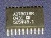
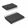
· Space-Saving 0.3" DIPs and 24- or 28-Terminal Surface Mount Packages
· Application Resistors On Chip for Gain Ranging, etc.
· Low Power LC2MOS
Application` Automatic Test Equipment
` Digital Attenuators
` Programmable Power Supplies
` Programmable Gain Amplifiers
` Digital-to-420 mA ConvertersSpecifications(TA = +25 unless otherwise stated)
VDD to DGND . . . . . . . . . . . . . . . . . . . . . ..0.3 V to +17 V
VSS to DGND . . . . . . . . . . . . . . . . . . . . . . .+0.3 V to 17 V
VREF to AGND . . . . . . . . . . . . . . . .VDD + 0.3 V, VSS 0.3 V
VRFB to AGND . . . . . . . . . . . . . . . .VDD + 0.3 V, VSS 0.3 V
VRA to AGND . . . . . . . . . . . . . . . . .VDD + 0.3 V, VSS 0.3 V
VRB to AGND . . . . . . . . . . . . . . . . .VDD + 0.3 V, VSS 0.3 V
VRC to AGND . . . . . . . . . . . . . . . . .VDD + 0.3 V, VSS 0.3 V
VOUT to AGND2 . . . . . . . . . . . . . . .VDD + 0.3 V, VSS 0.3 V
AGND to DGND . . . . . . . . . . . . . . . . . . . . . . . . . 0.3 V, VDD
Digital Input Voltage to DGND . . . . . 0.3 V to VDD + 0.3 V
Power Dissipation (Any Package)
To +75 . . . . . . . . . . . . . . . . . . . . . . . . . . . . . . . . 650 mW
Derates above +75 . . . . . . . . . . . . . . . . . . . . . 10 mW/
Operating Temperature Range
Commercial (J, K Versions) . . . . . . . . . . . . . . . 0 to +70
Industrial (A, B Versions) . . . . . . . . . . . . . . 40 to +85
Extended (S, T Versions) . . . . . . . . . . . . . . 55v to +125
Storage Temperature Range . . . . . . . . . . .65 to +150
Lead Temperature (Soldering, 10 sec) . . . . . . . . . . +300
NOTES
1Stresses above those listed under Absolute Maximum Ratings may cause permanent damage to the device. This is a stress rating only; functional operation of the device at these or any other conditions above those indicated in the operational sections of this specification is not implied. Exposure to absolute maximum rating conditions for extended periods of time may affect device reliability. Only one Absolute Maximum Rating may be applied at any one time.
2VOUT may be shorted to AGND provided that the power dissipation of the package is not exceeded.
DescriptionThe AD7845 is the industry's first 4-quadrant multiplying D/A converter with an on-chip amplifier. It is fabricated on the LC2MOS process, which allows precision linear components and digital circuitry to be implemented on the same chip.
The 12 data inputs drive latches which are controlled by standard CS and WR signals, making microprocessor interfacing simple. For stand-alone operation, the CS and WR inputs can be tied to ground, making all latches transparent. All digital inputs are TTL and 5 V CMOS compatible.
The output amplifier can supply ±10 V into a 2 kW load. It is internally compensated, and its input offset voltage is low due to laser trimming at wafer level. For normal operation, RFB is tied to VOUT, but the user may alternatively choose RA, RB or RC to scale the output voltage range.

 AD7845SE_883B_1371985 Data Sheet