Features: `Four 14-Bit DACs in One Package
AD7834-Serial Loading
AD7835-Parallel 8-/14-Bit Loading
`Voltage Outputs
`Power-On Reset Function
`Max/Min Output Voltage Range of +/8.192 V
`Maximum Output Voltage Span of 14 V
`Common Voltage Reference Inputs
`User Assigned Device Addressing
`Clear Function to User-Defined Voltage
`Surface Mount Packages
AD7834-28-Pin SO, DIP and Cerdip
AD7835-44-Pin PQFP and PLCCApplication·Process Control
·Automatic Test Equipment
·General Purpose InstrumentationPinout
 Specifications
VCC to DGND . . . . . . . . . . . . . . . 0.3 V, +7 V or VDD + 0.3 V
(Whichever Is Lower)
VDD to AGND . . . . . . . . . . . . . . . . . . . . . . . . . . 0.3 V, +17 V
VSS to AGND . . . . . . . . . . . . . . . . . . . . . . . . . . +0.3 V, 17 V
AGND to DGND . . . . . . . . . . . . . . .. . . . . . . . . 0.3 V, +0.3 V
Digital Inputs to DGND . . . . . . . . . . . . . . 0.3 V, VCC + 0.3 V
VREF(+) to VREF() . . . . . . . . . . . . . . . . . . . . . 0.3 V, +18 V
VREF(+) to AGND . . . . . . . . . . . . . . .VSS 0.3 V, VDD + 0.3 V
VREF() to AGND . . . . . . . . . . . . . .VSS 0.3 V, VDD + 0.3 V
DSG to AGND . . . . . . . . . . . . . . . . . VSS 0.3 V, VDD + 0.3 V
VOUT (14) to AGND . . . . . . . . . . . VSS 0.3 V, VDD + 0.3 V
Operating Temperature Range
Industrial (A Version) . . . . . . . . . . . . . .40°C to +85°C
Extended (S Version). . . . . . . . . . . . . .55°C to +125°C
Storage Temperature Range . . . . . . . . . 65°C to +150°C
Junction Temperature . . . . . . . . . . . . . . . . . . . . . . . +150°C
Plastic Package
JA Thermal Impedance . . . . . . . . . . . . . . . . . . . +75°C/W
Lead Temperature, Soldering (10 sec) . . . . . . . ..+260°C
Cerdip Package
JA Thermal Impedance . . . . . . . . . . . . . . . . . . . .+52°C/W
Lead Temperature, Soldering (10 sec) . . . . . . . . . +300°C
SOIC Package
JA Thermal Impedance . . . . . . . . . . . . . . . . . . . +75°C/W
Lead Temperature, Soldering
Vapor Phase (60 sec) . . . . . . . . . . . . . . . . . . . . +215°C
Infrared (15 sec) . . . . . . . . . . . . . . . . . . . . . . . . +220°C
PQFP Package
JA Thermal Impedance . . . . . . . . . . . . . . . . . . . . 95°C/W
Lead Temperature, Soldering
Vapor Phase (60 sec) . . . . . . . . . . . . . . . . . . . . .+215°C
Infrared (15 sec) . . . . . . . . . . . . . . . . . . . . . . . . +220°C
PLCC Package
JA Thermal Impedance. . . . . . . . . . . . . . . . . . . . +55°C/W
Lead Temperature, Soldering
Vapor Phase (60 sec) . . . . . . . . . . . . . . . . . . . . +215°C
Infrared (15 sec) . . . . . . . . . . . . . . . . . . . . . . . . . . .+220°C
Power Dissipation (Any Package) . . . . . . . . . . . . . . .480 mW
NOTES
1 Stresses above those listed under "Absolute Maximum Ratings" may cause permanent damage to the device. This is a stress rating only and functional operation of the device at these or any other conditions above those indicated in the operational section of this specification is not implied. Exposure to absolute maximum rating conditions for extended periods may affect device reliability.
2 Transient currents of up to 100 mA will not cause SCR latch up.
| Resolution (Bits) |
14bit |
| DAC Update Rate |
100kSPS |
| DAC Settling Time |
10s |
| # DAC Outputs |
4 |
| DAC Type |
Voltage Out |
| DAC Input Format |
Ser |
| Output FSR |
User Def. Range/Offset |
| Ref Int/Ext |
Ext |
| Supply Vnom |
Multi(±15, +5Dig) |
| Pwr Diss |
465mW |
| Package |
DIP,SOIC |
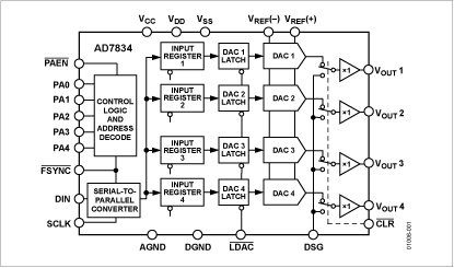
DescriptionThe AD7834 and AD7835 contain four 14-bit DACs on one monolithic chip. The AD7834 and AD7835 have output voltages in the range of ±8.192 V with a maximum span of 14 V.
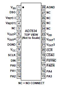
The AD7834 is a serial input device. Data is loaded in 16-bit format from the external serial bus, MSB first after two leading 0s, into one of the input latches via DIN, SCLK and FSYNC.The AD7834 has five dedicated package address pins, PA0PA4, that can be wired to AGND or VCC to permit up to 32 AD7834s to be individually addressed in a multipackage application.
The AD7835 can accept either 14-bit parallel loading or double-byte loading, where right-justified data is loaded in one 8-bit and one 6-bit byte. Data is loaded from the external bus into one of the input latches under the control of the WR, CS,BYSHF and DAC channel address pins, A0A2.
With either device, theLDAC signal can be used to update either all four DAC outputs simultaneously or individually, on reception of new data. In addition, for either device, the asynchronousCLR input can be used to set all signal outputs,VOUT1VOUT4, to the user-defined voltage level on the Device Sense Ground pin, DSG. On power-on, before the power supplies have stabilized, internal circuitry holds the DAC output voltage levels to within ±2 V of the DSG potential. As the supplies stabilize, the DAC output levels move to the exact DSG potential (assumingCLR is exercised).
The AD7834 is available in 28-pin 0.3" SO and 0.6" DIP packages,and the AD7835 is available in a 44-pin PQFP package and a 44-pin PLCC package.

 AD7834 Data Sheet