AD7740

Features: Synchronous OperationFull-Scale Frequency Set by External System Clock8-Lead SOT-23 and 8-Lead microSOIC Packages3 V or 5 V OperationLow Power: 3 mW (Typ)Nominal Input Range: 0 to VREFTrue 150 mV Capability Without Charge PumpVREF Range: 2.5 V to VDDInternal 2.5 V Reference1 MHz Max Inpu...

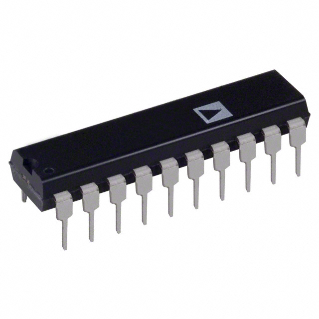
product image

AD7740 Picture
SeekIC No. : 004270780 Detail

AD7740: Features: Synchronous OperationFull-Scale Frequency Set by External System Clock8-Lead SOT-23 and 8-Lead microSOIC Packages3 V or 5 V OperationLow Power: 3 mW (Typ)Nominal Input Range: 0 to VREFTrue...

floor Price/Ceiling Price

Part Number:
AD7740
Supply Ability:
5000

Price Break

  • Qty
  • 1~5000
  • Unit Price
  • Negotiable
  • Processing time
  • 15 Days
Total Cost: $ 0.00

SeekIC Buyer Protection PLUS - newly updated for 2013!

  • Escrow Protection.
  • Guaranteed refunds.
  • Secure payments.
  • Learn more >>

Month Sales

268 Transactions

Rating

evaluate  (4.8 stars)

Upload time: 2024/11/21

Payment Methods

All payment methods are secure and covered by SeekIC Buyer Protection PLUS.

Notice: When you place an order, your payment is made to SeekIC and not to your seller. SeekIC only pays the seller after confirming you have received your order. We will also never share your payment details with your seller.
Product Details

Description


Features:

Synchronous Operation
Full-Scale Frequency Set by External System Clock
8-Lead SOT-23 and 8-Lead microSOIC Packages
3 V or 5 V Operation
Low Power: 3 mW (Typ)
Nominal Input Range: 0 to VREF
True 150 mV Capability Without Charge Pump
VREF Range: 2.5 V to VDD
Internal 2.5 V Reference
1 MHz Max Input Frequency
Selectable High Impedance Buffered Input
Minimal External Components Required
APPLICATIONS
Isolation of High Common-Mode Voltages
Low-Cost Analog-to-Digital Conversion
Battery Monitoring
Automotive Sensing


Application

  Connection Diagram


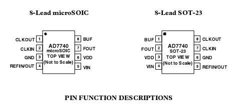
Pinout

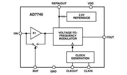
AD7740 Diagram


Specifications

VDD to GND . . . . . . . . . . . . . . . . . . . . . . . . . . . . . . . . . 0.3 V to +7 V
Analog Input Voltage to GND . . . . . . . . . . . . . . 0.3 V to VDD + 0.3 V
Reference Input Voltage to GND . . . . . . . . . . .. 0.3 V to VDD + 0.3 V
Logic Input Voltage to GND . . . . . . . . . . . . . . .. 0.3 V to VDD + 0.3 V
FOUT Voltage to GND . . . . . . . . . .. . . . . . . . . .. 0.3 V to VDD + 0.3 V
Operating Temperature Range
Commercial (K Version) . . . . . . . . . . . . . . . . . . . . . . . 0°C to +85°C
Automotive (Y Version) . . . . . . . . . . . . . . . . . . . . 40°C to +105°C
Storage Temperature Range . . . . . . . . . . . . . . . . 65°C to +150°C
Junction Temperature (TJ Max) . . . . . . . . . . . . . . . . . . . . . .. . . 150°C
SOT-23 Package
Power Dissipation . . . . . . . . . . . . . . . . . . . . . . . . . (TJ Max TA)/JA
JA Thermal Impedance . . . . . . . . . . . . . . . . . . . . . . . . . . . 240°C/W
Lead Temperature (10 secs) . . . . . . . . . . . . . . . . . . . .. . . . . . 300°C
Reflow Soldering
Peak Temperature . . . . . . . . . . . . . . . . . . . . . . . . . . . . . 220 + 5/0°C
Time at Peak Temperature . . . . . 10 sec to 40 secmicroSOIC Package
Power Dissipation . . . . . . . . . . . . . . . . . . . . . . . . . . (TJ Max TA)/JA
JA Thermal Impedance . . . . . . . . . . . . . . . . . . . . . . . . . . . 206° C/W
JC Thermal Impedance . . . . . . . . . . . . . . . . . . . . . . . . . . . . 44° C/W
Lead Temperature (10 secs) . . . . . . . . . . . . . . . . . . . . . . . . . 300 °C
Reflow Soldering
Peak Temperature . . . . . . . . . . . . . . . . . . . . . . . . . . . . 220 +5/0 °C
Time at Peak Temperature . . . . . . . . . . . . . . . . . . . . 10 sec to 40 sec


Architecture Synchronous
# Channels 1-Single Ended
Input Voltage Range (V) +2.5V
Full Scale Fout (kHz) 500kHz
Reference Voltage (V) 2.5V
Accuracy (%/kHz) 1
Input Clk Frequency (MHz) 1MHz
Voltage Supply (V) 3 to 5.25
Supply Current 1.5mA
Package 8-Lead MSOP,8-Lead SOT-23


Description

The AD7740 is a low-cost, ultrasmall synchronous Voltage-to-Frequency Converter (VFC). It works from a single 3.0 V to 3.6 V or 4.75 V to 5.25 V supply consuming 0.9 mA. The AD7740 is available in an 8-lead SOT-23 and also in an 8-lead microSOIC package. Small package, low cost and ease of use were major design goals for this product. The part contains an on-chip 2.5 V bandgap reference but the user may overdrive this using an
external reference. This external reference range includes VDD.

The full-scale output frequency is synchronous with the clock signal on the CLKIN pin. This clock can be generated with the addition of an external crystal (or resonator) or supplied from a CMOS-compatible clock source. The part has a maximum input frequency of 1 MHz. For an analog input signal that goes from 0 V to VREF, the out-put frequency goes from 10% to 90% of fCLKIN. In buffered mode,the part provides a very high input impedance and accepts a range of 0.1 V to VDD 0.2 V on the VIN pin.

There is also an unbuffered mode of operation that allows VIN to go from0.15 V to VDD + 0.15 V. The modes are interchangeable using the BUF pin. The AD7740 (Y Grade) is guaranteed over the automotive temperature range of 40°C to +105°C. The AD7740 (K Grade) is guaranteed from 0°C to 85°C.


Customers Who Bought This Item Also Bought

Margin,quality,low-cost products with low minimum orders. Secure your online payments with SeekIC Buyer Protection.
Optical Inspection Equipment
RF and RFID
Sensors, Transducers
Transformers
Computers, Office - Components, Accessories
View more