Features: AD7705: Two Fully Differential Input Channel ADCs
AD7706: Three Pseudo Differential Input Channel ADCs
16 Bits No Missing Codes
0.003% Nonlinearity
Programmable Gain Front End
Gains from 1 to 128
Three-Wire Serial Interface
SPI(TM), QSPI(TM), MICROWIRE(TM) and DSP Compatible
Schmitt Trigger Input on SCLK
Ability to Buffer the Analog Input
2.7 V to 3.3 V or 4.75 V to 5.25 V Operation
Power Dissipation 1 mW max @ 3 V
Standby Current 8 mA max
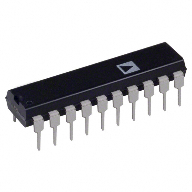
16-Lead DIP, 16-Lead SOIC and TSSOP Packages
Pinout SpecificationsVDD to GND . . . . . . . . . . . . . . . . . . . . . . . . . . .0.3V to +7 V
Analog Input Voltage to GND . . . . . . . 0.3 V to VDD + 0.3 V
Reference Input Voltage to GND . . . . 0.3 V to VDD + 0.3 V
Digital Input Voltage to GND . . . . . . . .0.3 V to VDD + 0.3 V
Digital Output Voltage to GND . . . . . .0.3 V to VDD + 0.3 V
Operating Temperature Range
Commercial (B Version) . . . . . . . . . . . . . . .40 °C to +85°C
Storage Temperature Range . . . . . . . . . 65°C to +150 °C
Junction Temperature . . . . . . . . . . . . . . . . . . . . . . +150 °C
Plastic DIP Package, Power Dissipation . . . . . . . . .450 mW
q JA Thermal Impedance . . . . . . . . . . . . . . . . . . . .105 C/W
Lead Temperature, (Soldering, 10 sec) . . . . . . . . +260 °C
SOIC Package, Power Dissipation . . . . . . . . . . . . .450 mW
q JA Thermal Impedance . . . . . . . . . . . . . . . . . . . . .75 C/W
Lead Temperature, Soldering
Vapor Phase (60 sec) . . . . . . . . . . . . . . . . .. . . . +215 °C
Infrared (15 sec) . . . . . . . . . . . . . . . . . . . . . . . . . .+220 °C
SSOP Package, Power Dissipation . . . . . . . . . . . . .450 mW
q JA Thermal Impedance . . . . . . . . . . . . . . . . . . . 139 C/W
Lead Temperature, Soldering
Vapor Phase (60 sec) . . . . . . . . . . . . . . . . . . . . . +215 °C
Infrared (15 sec) . . . . . . . . . . . . . . . . . . . . . . . . . .+220°C
ESD Rating . . . . . . . . . . . . . . . . . . . . . . . . . . . . . .>4000 V
| Resolution (Bits) |
16bit |
| T-Put Rate |
500SPS |
| # Chan |
3 |
| Supply V |
Single(+3),Single(+5) |
| Pwr Diss |
6.5mW |
| Interface |
Ser,SPI |
| Ain Range |
Bip (Vref)/(PGA Gain),Uni (Vref)/(PGA Gain) |
| SNR (dB) |
116dB |
| Pkg Type |
DIP,SOIC,SOP |
DescriptionThe AD7705/AD7706 are complete analog front ends for low frequency measurement applications. These two-/three-channel devices can accept low level input signals directly from a transducer and produce a serial digital output. They employ a sigmadelta conversion technique to realize up to 16 bits of no missing codes performance. The selected input signal is applied to a proprietary programmable gain front end based around an analog modulator. The modulator output is processed by an onchip digital filter. The first notch of this digital filter can be programmed via an on-chip control register allowing adjustment of the filter cutoff and output update rate.
The AD7705/AD7706 operate from a single 2.7 V to 3.3 V or 4.75 V to 5.25 V supply. The AD7705 features two fully differential analog input channels while the AD7706 features three pseudo differential input channels. Both devices feature a differential reference input. Input signal ranges of 0 mV to +20ÊmV through 0 V to +2.5ÊV can be incorporated on both devices when operating with a VDD of 5 V and a reference of 2.5 V. They can also handle bipolar input signal ranges of ±20ÊmV through ±2.5ÊV, which are referenced to the AIN() inputs on the AD7705 and to the COMMON input on the AD7706. The AD7705/AD7706, with 3 V supply and a 1.225 V reference, can handle unipolar input signal ranges of 0 mV to +10ÊmV through 0 V to +1.225ÊV. Its bipolar input signal ranges are ±10ÊmV through ±1.225ÊV.
The AD7705/AD7706 thus perform all signal conditioning and conversion for a two- or three-channel system.
The AD7705/AD7706 are ideal for use in smart, microcontroller or DSP-based systems. They feature a serial interface that can be configured for three-wire operation. Gain settings, signal polarity and update rate selection can be configured in software using the input serial port. The part contains self-calibration and system calibration options to eliminate gain and offset errors on the part itself or in the system.
CMOS construction ensures very low power dissipation, and the power-down mode reduces the standby power consumption to 20ÊmW typ. These parts are available in a 16-lead, 0.3 inch-wide, plastic dual-in-line package (DIP), a 16-lead wide body (0.3 inch) small outline (SOIC) package and also a low profile 16- lead TSSOP.

 AD7706 Data Sheet


