Features: 2 s ADC with Track/Hold
1 s DAC with Output Amplifier
AD7569, Single DAC Output
AD7669, Dual DAC Output
On-Chip Bandgap Reference
Fast Bus Interface
Single or Dual 5 V SuppliesPinout Specifications
VDD to AGNDDAC or AGNDADC . . . . . . . . . . . . .0.3 V, +7 V
VDD to DGND . . . . . . . . . . . . . . . . . . . . . . . . . .0.3 V, +7 V
VDD to VSS . . . . . . . . . . . . . . . . . . . . . . . . . . .0.3 V, +14 V
AGNDDAC or AGNDADC to DGND . . . . . . 0.3 V, VDD + 0.3 V
AGNDDAC to AGNDADC . . . . . . . . . . . . . . . . . . . . . . . . .±5 V
Logic Voltage to DGND . . . . . . . . . . . . .0.3 V, VDD + 0.3 V
CLK Input Voltage to DGND . . . . . . . . . 0.3 V, VDD + 0.3 V
VOUT (VOUTA, VOUTB) to
AGND1DAC . . . . . . . . . .. . . . .. . . . VSS 0.3 V, VDD + 0.3 V
VIN to AGNDADC . . . . . . . . . . . . . . .VSS 0.3 V, VDD + 0.3 V
Power Dissipation (Any Package) to +75 . . . . . . . 450 mW
Derates above 75by . . . . . . . . . . . . . . . . . . . . . . 6 mW/
Operating Temperature Range
Commercial (J, K) . . . . . . . . . . . . . . . . . . . . . . . .0 to +70
Industrial (A, B) . . . . . . . . . . . . . . . . . . . . .. 40 to +85
Extended (S, T) . . . . . . . . . . . . . . . . . . . . . 55 to +125
Storage Temperature Range . . . . . . . . . . . 65 to +150
Lead Temperature (Soldering, 10 secs) . . . . . . . . . . . +300
DescriptionThe AD7569/AD7669 is a complete, 8-bit, analog I/O systemon a single monolithic chip. The AD7569 contains a high speedsuccessive approximation ADC with 2 s conversion time, a track/hold with 200 kHz bandwidth, a DAC and an output buffer ampli-fier with 1 s settling time. A temperature-compensated 1.25 Vbandgap reference provides a precision reference voltage for theADC and the DAC. The AD7669 is similar, but contains twoDACs with output buffer amplifiers.
A choice of analog input/output ranges is available. Using a sup-ply voltage of +5 V, input and output ranges of zero to 1.25 Vand zero to 2.5 volts may be programmed using the RANGE in-put pin. Using a ±5 V supply, bipolar ranges of ±1.25 V or±2.5 V may be programmed.
Digital interfacing is via an 8-bit I/O port and standard micro-processor control lines. Bus interface timing is extremely fast, al-lowing easy connection to all popular 8-bit microprocessors. Aseparate start convert line controls the track/hold and ADC togive precise control of the sampling period.
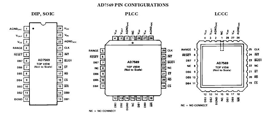
The AD7569/AD7669 is fabricated in Linear-CompatibleCMOS (LC2MOS), an advanced, mixed technology processcombining precision bipolar circuits with low power CMOSlogic. The AD7569 is packaged in a 24-pin, 0.3" wide "skinny"DIP, a 24-terminal SOIC and 28-terminal PLCC and LCCCpackages. The AD7669 is available in a 28-pin, 0.6" plasticDIP, 28-terminal SOIC and 28-terminal PLCC package.

 AD7669 Data Sheet


