Features: ·On-Chip Latches for Both DACs
·+12 V to +15 V Operation
·DACs Matched to 1%
·Four Quadrant Multiplication
·TTL/CMOS Compatible from +12 V to +15 V
·Latch Free (Protection Schottkys not Required)
Application·Disk Drives
·Programmable Filters
·X-Y Graphics
·Gain/Attenuation
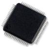
Pinout Specifications
VDD to AGND . . . . . . . . . . . . . . . . . . . . . . . . . .0 V, +17 V
VDD to DGND . . . . . . . . . . . . . . . . . . . . . . . . . . 0 V, +17 V
AGND to DGND . . . . . . . . . . . . . . . . . . . . . . . .VDD + 0.3 V
DGND to AGND . . . . . . . . . . . . . . . . . . . . . . . .VDD + 0.3 V
Digital Input Voltage to DGND . . . . . .0.3 V, VDD + 0.3 V
VPIN2, VPIN20 to AGND . . . . . . . . . . . 0.3 V, VDD + 0.3 V
VREF A, VREF B to AGND . . . . . . . . . . . . . . . . . . . . . ±25 V
VRFB A, VRFB B to AGND . . . . . . . . . . . . . . . . . . . . . ±25 V
Power Dissipation (Any Package) to +75°C . . . . 450 mW
Derates above +75°C by . . . . . . . . . . . . . . . 6 mW/°C
Operating Temperature Range
Commercial (K) Grades . . . . . . . . . . . . 40°C to +85°C
Industrial (B) Grades . . . . . . . . . . . . .. 40°C to +85°C
Extended (T) Grades . . . . . . . . . . . . .55°C to +125°C
Storage Temperature . . . . . . . . . . . . . .65°C to +150°C
Lead Temperature (Soldering, 10 sec) . . . . . . . . . +300°C
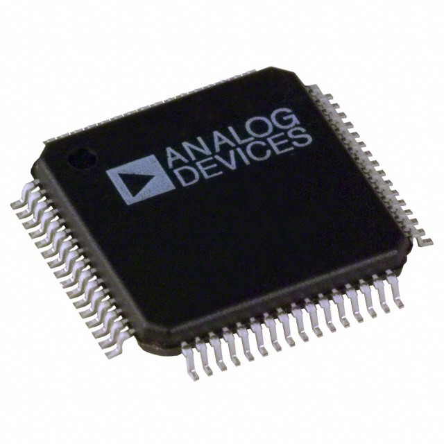
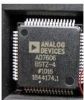
DescriptionThe AD7628 is a monolithic dual 8-bit digital/analog converter featuring excellent DAC-to-DAC matching. It is available in small 0.3" wide 20-pin DIPs and in 20-terminal surface mount packages.
Separate on-chip latches are provided for each DAC to allow easy microprocessor interface.
Data is transferred into either of the two DAC data latches via a common 8-bit TTL/CMOS compatible input port. Control input DAC A/DAC B determines which DAC is to be loaded. The AD7628's load cycle is similar to the write cycle of a random access memory, and the device is bus compatible with most 8-bit microprocessors, including 6502, 6809, 8085, Z80.
The device operates from a +12 V to +15 V power supply and is TTL-compatible over this range. Power dissipation is a low 20 mW.
Both DACs offer excellent four quadrant multiplication characteristics with a separate reference input and feedback resistor for each DAC.

 AD7628 Data Sheet