DescriptionThe AD7572A is a kind of enhanced replacement for the industry standard AD7572. The device is a kind of complete 12-bit ADC that offers high speed performance combined with low, CMOS power levels. The device has a high speed digital interface with three-state data outputs and can operate under the control of standard microprocessor Read (RD) and decoded address (CS) signals. Interface timing is sufficiently fast to allow the AD7572A to operate with most microprocessors, with three-state enable times of only 90 ns and bus relinquish times of 75 ns. The device is fabricated in analog devices linear compatible CMOS process (LC2MOS), an advanced all ion-implanted process that combines fast CMOS logic and linear, bipolar circuits on a single chip, thus achieving excellent linear performance while retaining low CMOS power levels.
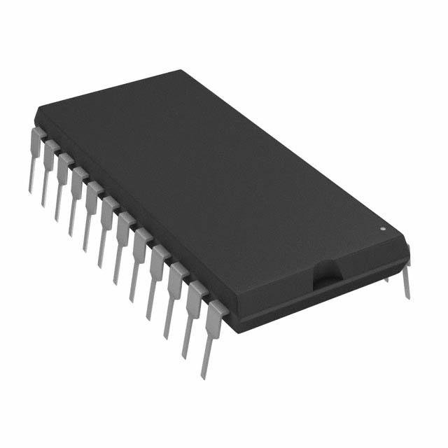
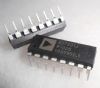
There are some features as follows: (1)improved AD7572; (2)faster conversion time: AD7572AXX03: 3s; AD7572AXX10: 10s; (3)5 V and -12 V or -15 V power supply operation; (4)better offset and gain error specifications; (5)extended plastic temperature range (-40 to +85) ; (6)low power: 100 mW; (7)small 24-pin, 0.3" wide DIP and SOIC DIP package.
The last one is about the absolute maximum ratings (Ta=+25 unless otherwise noted) of AD7572A: (1)VDD to DGND: -0.3 to +7 V; (2)VSS to DGND: +0.3 to -17 V; (3)AGND to DGND: -0.3 to VDD+0.3 V; (4)AIN to AGND: -15 to +15 V; (5)digital input voltage to DGND (CLK IN, HEBEN, RD, CS): -0.3 to VDD+0.3 V; (6)digital output voltage to DGND (D11-D0/8, CLK OUT, BUSY): -0.3 to VDD+0.3 V; (7)power dissipation: 1000 mW (any package) to 75; (8)operating temperature range: commercial (J, L versions): 0 to +70; industrial (A version): -40 to +85; extended (S version): -65 to 150; (9)storage temperature: -65 to 150; (10)lead temperature (soldering, 10secs): +300.

 AD7572A Data Sheet