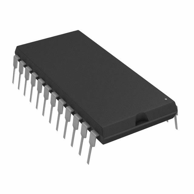
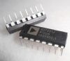
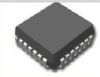
Pinout Specifications
| Resolution (Bits) |
12bit |
| DAC Update Rate |
667kSPS |
| DAC Settling Time |
1.5s |
| # DAC Outputs |
2 |
| DAC Type |
Current Out |
| DAC Input Format |
Nibble |
| Output FSR |
(-Vref),(Bip Vref) |
| Ref Int/Ext |
Ext |
| Supply Vnom |
Single(+15) |
| Pwr Diss |
75mW |
| Package |
DIP,LCC |
DescriptionThe AD7549 is a kind of monolithic dual, 12-bit, current output D/A converter. The device is available in both 0.3" wide 20-pin DIPs and in 20-terminal surface mount packages. Both DACs provide four quadrant multiplication capabilities with a seperate reference input and feedback resistor for each DAC. The monolithic construction ensures excellent thermal tracking and gain error tracking between the two DACs. The device is manufactured using the linear compatible CMOS process. It is speed compatible with most microprocessors and accepts TTL, 74HC or 5 V CMOS logic level inputs. The typical applications include: (1)programmable filters; (2)automatic test equipment; (3)microcomputer based process control; (4)audio systems; (5)programmable power supplies; (6)synchro applications.
There are some features of AD7549 as follows: (1)two doubled buffered 12-bit DACs; (2)4-quadrant multiplication; (3)low gain error (3LSBs max); (4)DAC ladder resistance matching: 1%; (5)space saving skinny DIP and surface mount packages; (6)latch-up proof; (7)extended temperature range operation.
The last one is about the absolute maximum ratings (Ta=+25 unless otherwise noted) of AD7549: (1)VDD (pin 20) to DGND: -0.3 to +17 V; (2)VREFA, VREFB (pins 19, 13) to AGND: ±25 V; (3)VREBA, VRFBB (pins 19, 13) to AGND: ±25 V; (4)digital input voltage (pins 1-11) to DGND: -0.3 to VDD+0.3 V; (5)VPIN15, VPIN17, to DGND: -0.3 to VDD+0.3 V; (6)AGND to DGND: -0.3 to VDD+0.3 V; (7)power dissipation (any package): 450 mW to +75; (8)operating temperature range: commercial (J, K versions): -40 to +85; industrial (A, B versions): -40 to +85; extended (S, T versions): -65 to 150; (9)storage temperature: -65 to 150; (10)lead temperature (soldering, 10secs): +300.
The AD7549 is a monolithic dual, 12-bit, current output D/A converter. It is packaged in both 0.3" wide 20-pin DIPs and in 20-terminal surface mount packages. Both DACs provide four quadrant

 AD7549 Data Sheet