Features: SpecificationsDescriptionThe AD75069 is designed as monolithic octal 12-bit DACPORTs which contain eight complete 12-bit, voltage output digital to analog converters in one monolithic IC. It offer the highest density 12-bit DA/functions available. Typical applications include automatic t...
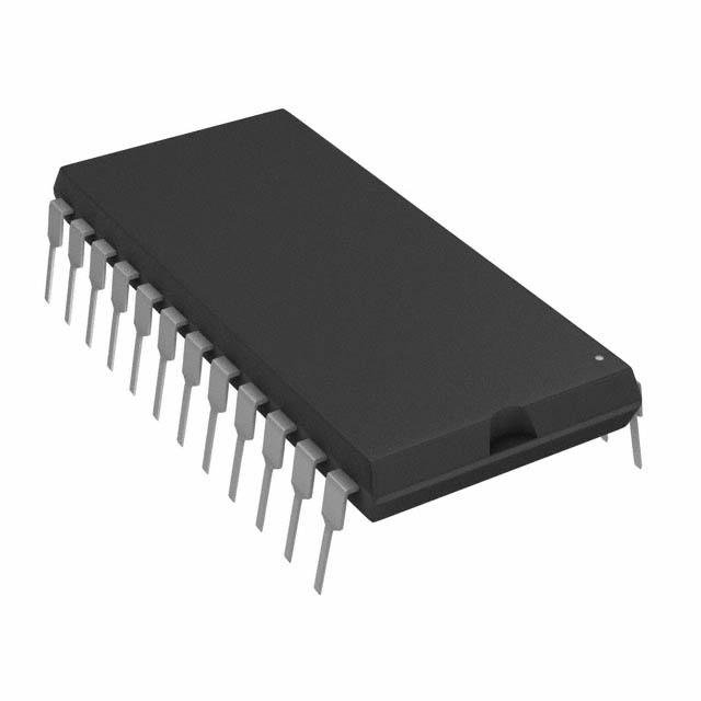
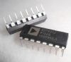
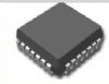
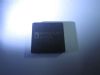
AD75069: Features: SpecificationsDescriptionThe AD75069 is designed as monolithic octal 12-bit DACPORTs which contain eight complete 12-bit, voltage output digital to analog converters in one monolithic IC. ...
SeekIC Buyer Protection PLUS - newly updated for 2013!
268 Transactions
All payment methods are secure and covered by SeekIC Buyer Protection PLUS.
The AD75069 is designed as monolithic octal 12-bit DACPORTs which contain eight complete 12-bit, voltage output digital to analog converters in one monolithic IC. It offer the highest density 12-bit DA/functions available. Typical applications include automatic test equipment, instrumentation, avionics, robotics, process control.
AD75069 has five features. The first one is eight complete voltage output DACs. The second one is on-chip voltage reference. The third one is on-chip data latches with readback feature. The fourth one is variety of output voltage ranges +7.5V / -2.5V, +/-5V, +/-10V. The fifth one is compact 44-pin PLCC and ceramic JLCC packages. That are all the main features.
Some absolute maximum ratings of AD75069 have been concluded into several points as follow. The first one is about its Vcc to DGND or IOGND which would be from 0V to +7V. The second one is about its Vdd to AGND which would be from 0V to +18V. The third one is about its Vss to AGND which would be from -18V to 0V. The fourth one is about its AGND to DGND which would be from -1V to +1V. The fifth one is about its AGND to VREFGND which would be +/-13.2V. The sixth one is about its AGND to VRET0-7 which would be +/-13.2V. The seventh one is about its Vrefin input which would be from Vdd to Vss. The eighth one is about its Vdd to Vss which would be from 0V to +26.4V. The ninth one is about its digital inputs which would be from -0.3V to +7V. The tenth one is about its analog outputs which means indefinite shorts to Vcc, Vdd, Vss and AGND. The eleventh one is about its soldering temperature which would be +300°C, 10sec. The twelfth one is about its power dissipation which would be 1000mW. It should be noted that stresses above listed under absolute maximum ratings may cause permanent damage to the device. And so on. For more information please contact us.