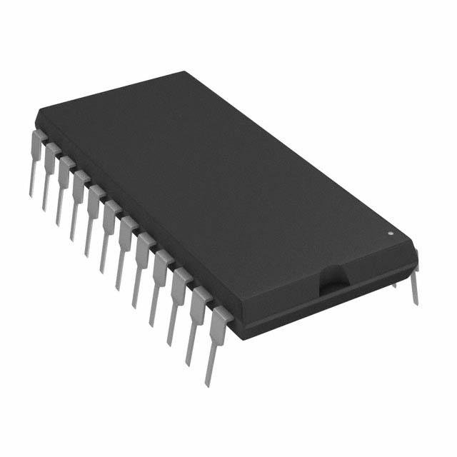
Features: ` 256 Switches in a 16 *16 Array` Wide Signal Range: to Supply Rails of 24 V or 612 V` Low On-Resistance: 200 Typ` TTL/CMOS/Microprocessor-Compatible Control Lines` Serial Input Simplifies Interface` Serial Output Allows Cascading for More Channels` Low Power Consumption: 2 mW Quiescent`...
AD75019: Features: ` 256 Switches in a 16 *16 Array` Wide Signal Range: to Supply Rails of 24 V or 612 V` Low On-Resistance: 200 Typ` TTL/CMOS/Microprocessor-Compatible Control Lines` Serial Input Simplifies...
SeekIC Buyer Protection PLUS - newly updated for 2013!
268 Transactions
All payment methods are secure and covered by SeekIC Buyer Protection PLUS.
Min | Max | Units | Conditions | |
VDD to DGND VSS to DGND VCC to DGND VDD to VSS VCC to VSS Digital Inputs to DGND Power Dissipation Operating Temperature Range Storage Temperature Lead Temperature |
0.5 25.2 0.5 0.5 0.5 - 0.5 0 -65 |
+25.2 +0.5 +7.0 +25.2 +25.2 VCC + 0.5 1.0 +70 +150 +300 |
V V V V V V sec W |
TA 75°C Soldering, 10 sec |
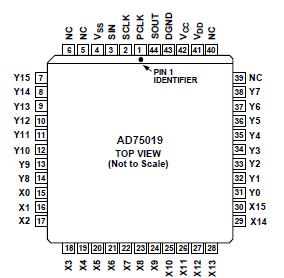
The AD75019 contains 256 analog switches in a 16*16 array. Any of the X or Y pins may serve as an input or output. Any or all of the X terminals may be programmed to connect to any or all of the Y terminals. The switches can accommodate signals with amplitudes up to the supply rails and have a typical onresistance of 150 .
Data is loaded serially via the SIN input and clocked into an onboard 256-bit shift register via SCLK. When all the switch settings have been programmed, data is transferred into a set of 256 latches via PCLK. The serial shift register is dynamic, so there is a minimum clock rate of 20 kHz. The maximum clock rate of 5 MHz allows loading times as short as 52 s. The switch control latches AD75019 are static and will hold their data as long as power is applied.
To extend the number of switches in the array, you may cascade multiple AD75019s. The SOUT output is the end of the shift register, and may be connected to the SIN input of the next AD75019.
The AD75019 is fabricated in Analog Devices' BiMOS II process. This epitaxial BiCMOS process features CMOS devices for low distortion switches and bipolar devices for ESD protection.