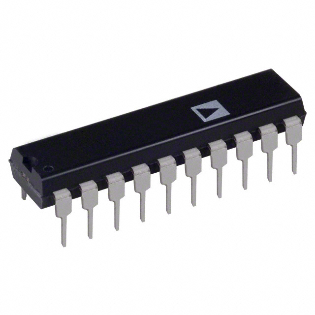
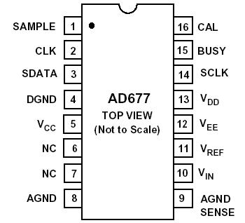
Features: `Autocalibrating`On-Chip Sample-Hold Function`Serial Output`16 Bits No Missing Codes`61 LSB INL`99 dB THD`92 dB S/(N+D)`1 MHz Full Power BandwidthPinoutSpecifications Resolution (Bits) 16bit T-Put Rate 100kSPS # Chan 1 Supply V Multi(±12, +5) Pwr Diss 630mW ...
AD677: Features: `Autocalibrating`On-Chip Sample-Hold Function`Serial Output`16 Bits No Missing Codes`61 LSB INL`99 dB THD`92 dB S/(N+D)`1 MHz Full Power BandwidthPinoutSpecifications Resolution (Bi...
SeekIC Buyer Protection PLUS - newly updated for 2013!
268 Transactions
All payment methods are secure and covered by SeekIC Buyer Protection PLUS.
Resolution (Bits) | 16bit |
T-Put Rate | 100kSPS |
# Chan | 1 |
Supply V | Multi(±12, +5) |
Pwr Diss | 630mW |
Interface | Ser |
Ain Range | Bip (Vref) |
SNR (dB) | n/a |
Pkg Type | DIP,SOIC |
VCC to VEE . . . . . . . . . . . . . . . . . . . . . . . . . .0.3 V to +26.4 V
VDD to DGND . . . . . . . . . . . . . . . . . . . . . . . . . . 0.3 V to +7 V
Vcc to AGND . . . . . . . . . . . . . . . . . . . . . . . . . .0.3 V to +18 V
VEE to AGND . . . . . . . . . . . . . . . . . . . . . . . . . .18 V to +0.3 V
AGND to DGND . . . . . . . . . . . . . . . . . . . . . . . . . . . . . . . +0.3 V
Digiul Inputs to DGND . . . . . . . . . . . . . . . . . . . . . . 0 to +5.5 V
Analog Inputs, VREF to AGND
. . . . . . . . . . . . . . . . . . . . . . . . . . (VCC +0.3 V) to (VEE 0.3 V)
Soldering . . . . . . . . . . . . . . . . . . . . . . . . . . . +300°C, 10 sec
Storage Temperature . . . . . . . . . . . . . . . 65°C to +150°C
*Stresses greater than those listed under "Absolute Maximum Ratings" may cause permanent damage to the device. This is a stress rating only and functional operation of the device at these or any other conditions above those indicated in the operational section of this specification is not implied. Exposure to absolute maximum rating conditions for extended periods may affect device reliability.
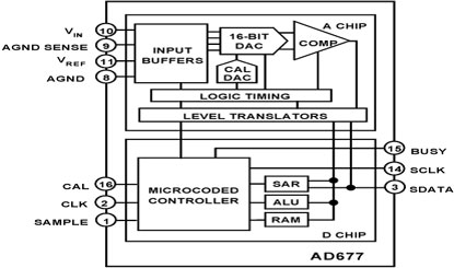
The AD677 is a multipurpose 16-bit serial output analog-todigital converter which utilizes a switched-capacitor/charge redistribution architecture to achieve a 100 kSPS conversion rate (10 ms total conversion time). Overall performance is optimized by digitally correcting internal nonlinearities through on-chip autocalibration.
The AD677 circuitry is segmented onto two monolithic chips- a digital control chip fabricated on Analog Devices DSP CMOS process and an analog ADC chip fabricated on our BiMOS II process. Both chips are contained in a single package.
The AD677 is specified for ac (or "dynamic") parameters such as S/(N+D) Ratio, THD and IMD which are important in signal processing applications. In addition, dc parameters are specified which are important in measurement applications.
The AD677 operates from +5 V and ±12 V supplies and typically consumes 450 mW using a 10 V reference (360 mW with 5 V reference) during conversion. The digital supply (VDD) is separated from the analog supplies (VCC, VEE) for reduced digital crosstalk. An analog ground sense is provided to remotely sense the ground potential of the signal source. This can be useful if the signal has to be carried some distance to the A/D converter. Separate analog and digital grounds are also provided.
The AD677 is available in a 16-pin narrow plastic DIP, 16-pin narrow side-brazed ceramic package, or 28-lead SOIC. A parallel output version, the AD676, is available in a 28-pin ceramic or plastic DIP. All models operate over a commercial temperature range of 0°C to +70°C or an industrial range of 40°C to +85°C.