AD668

Features: Ultrahigh Speed: Current Settling to 1 LSB in 90 ns fora Full-Scale Change in Digital Input. Voltage Settlingto 1 LSB in 120 ns for a Full-Scale Change in AnalogInput15 MHz Reference BandwidthMonotonicity Guaranteed over Temperature10.24 mA Current Output or 1.024 V Voltage OutputIntegra...

product image

AD668 Picture
SeekIC No. : 004269774 Detail

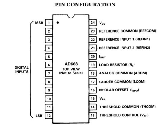
AD668: Features: Ultrahigh Speed: Current Settling to 1 LSB in 90 ns fora Full-Scale Change in Digital Input. Voltage Settlingto 1 LSB in 120 ns for a Full-Scale Change in AnalogInput15 MHz Reference Bandw...

floor Price/Ceiling Price

Part Number:
AD668
Supply Ability:
5000

Price Break

  • Qty
  • 1~5000
  • Unit Price
  • Negotiable
  • Processing time
  • 15 Days
Total Cost: $ 0.00

SeekIC Buyer Protection PLUS - newly updated for 2013!

  • Escrow Protection.
  • Guaranteed refunds.
  • Secure payments.
  • Learn more >>

Month Sales

268 Transactions

Rating

evaluate  (4.8 stars)

Upload time: 2024/6/9

Payment Methods

All payment methods are secure and covered by SeekIC Buyer Protection PLUS.

Notice: When you place an order, your payment is made to SeekIC and not to your seller. SeekIC only pays the seller after confirming you have received your order. We will also never share your payment details with your seller.
Product Details

Description


Features:

Ultrahigh Speed: Current Settling to 1 LSB in 90 ns fora Full-Scale Change in Digital Input. Voltage Settlingto 1 LSB in 120 ns for a Full-Scale Change in AnalogInput
15 MHz Reference Bandwidth
Monotonicity Guaranteed over Temperature
10.24 mA Current Output or 1.024 V Voltage Output
Integral and Differential Linearity Guaranteed over
Temperature
0.3" "Skinny DIP" Packaging
MIL-STD-883 Compliant Versions Available


Pinout

  Connection Diagram


Specifications

VCC to REFCOM  . . . . . . . . . . . . . . . . . . . . . . . . 0 V to +18 V
VEE to REFCOM . . . . . . . . . . . . . . . . . . . . . . . . .0 V to 18 V
REFCOM to LCOM . . . . . . . . . . . . . . . . . . +100 mV to 10 V
ACOM to LCOM  . . . . . . . . . . . . . .  . . . . . . . . . . . . ±100 mV
THCOM to LCOM . . . . . . . . . . . . . . . . . . . . . . . . . . ±500 mV
REFCOM to REFIN (1, 2)  . . . . . . . . . . . . . . . . . . . . . . . .18 V
IBPO to LCOM  . . . . . . . . . . . . . . . . . . . . .. . . . . . . . . . .±5 V
IOUT to LCOM . . . . . . . . . . . . . . . . . . . . .. . . . . . 5 V to VTH
Digital Inputs to THCOM . . . . . . . . . . .. . 500 mV to +7.0 V
REFIN1 to REFIN2  . . . . . . . . . . . . . . . . . . . . . . . . . . . . .36 V
VTH to THCOM  . . . . . . . . . . . . . . . . . . . . .  0.7 V to +1.4 V
Logic Threshold Control Input Current  . . . .  . . . . . . . . 5 mA
Power Dissipation  . . . . . . . . . . . . . . . . . . . . . . . . . .670 mW
Storage Temperature Range
Q (Cerdip) Package  . . . . . . . . . . . . . . . . . .65 to +150
Junction Temperature  . . . . . . . . . . . . . . . . . . . . . . . +175
Thermal Resistance
JA  . . . . . . . . . . . . . . . . . . . . . . . . . . . . . . . . . . . . . +75/W
JC  . . . . . . . . . . . . . . . . . . . . . . . . . . . . . . . . . . . . . +25/W


Description

The AD668 is an ultrahigh speed, 12-bit, multiplying digital-to-analog converter, providing outstanding accuracy and speed per-formance in responding to both analog and digital inputs. TheAD668 provides a level of performance and functionality in amonolithic device that exceeds that of many contemporary hy-brid devices. The part is fabricatedusing Analog Devices'Complementary Bipolar (CB) Process, which features verticalNPN and PNP devices on the same chip without the use ofdielectric isolation. The AD668's design capitalizes on this pro-prietary process in combination with standard low impedancecircuit techniques to provide its unique combination of speedand accuracy in a monolithicpart.

The wideband reference input is buffered by a high gain, closedloop reference amplifier. The reference input is essentially a 1 V,high impedance input, but trimmed resistive dividers are pro-vided to readily accommodate 5 V and 1.25 V references. Thereference amplifier features an effective small signal bandwidthof 15 MHz and an effective slew rate of 3% of full scale/ns.

Multiple matched current sources and thin film ladder tech-niques are combined to produce bit weighting. The output rangecan nominally be taken as a 10.24 mA current output or a 1.024 Vvoltage output. Varying the analog input can provide modulationof the DAC full scale from 10% to 120% of its nominal value.Bipolar outputs can be realized through pin-strapping to providetwo-quadrant operation without additional external circuitry.

Laser wafer trimming insures full 12-bit linearity and excellentgain accuracy. All grades of the AD668 are guaranteed mono-tonic over their full operating temperature range. Furthermore,the output resistance of the DAC is trimmed to 100± 1.0%.

The AD668 is available in four performance grades. TheAD668JQ and KQ are specified for operation from 0 to+70, the AD668AQ is specified for operation from 40 to+85, and the AD668SQ specified for operation from 55to +125. All grades are available in a 24-pin cerdip (0.3"package.


Customers Who Bought This Item Also Bought

Margin,quality,low-cost products with low minimum orders. Secure your online payments with SeekIC Buyer Protection.
Cable Assemblies
Memory Cards, Modules
Line Protection, Backups
Discrete Semiconductor Products
Static Control, ESD, Clean Room Products
View more