AD667

Features: Complete 12-Bit D/A FunctionDouble-Buffered LatchOn Chip Output AmplifierHigh Stability Buried Zener Reference Single Chip Construction Monotonicity Guaranteed Over Temperature Linearity Guaranteed Over Temperature: 1/2 LSBPinoutSpecificationsVCCto Power Ground . . . . . . . . . . . . ....

product image

AD667 Picture
SeekIC No. : 004269770 Detail

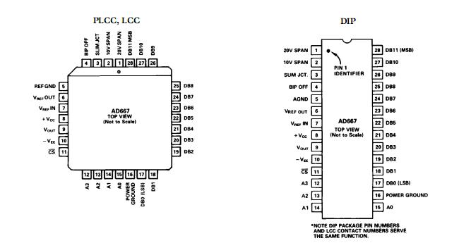
AD667: Features: Complete 12-Bit D/A FunctionDouble-Buffered LatchOn Chip Output AmplifierHigh Stability Buried Zener Reference Single Chip Construction Monotonicity Guaranteed Over Temperature Linearity ...

floor Price/Ceiling Price

Part Number:
AD667
Supply Ability:
5000

Price Break

  • Qty
  • 1~5000
  • Unit Price
  • Negotiable
  • Processing time
  • 15 Days
Total Cost: $ 0.00

SeekIC Buyer Protection PLUS - newly updated for 2013!

  • Escrow Protection.
  • Guaranteed refunds.
  • Secure payments.
  • Learn more >>

Month Sales

268 Transactions

Rating

evaluate  (4.8 stars)

Upload time: 2024/6/9

Payment Methods

All payment methods are secure and covered by SeekIC Buyer Protection PLUS.

Notice: When you place an order, your payment is made to SeekIC and not to your seller. SeekIC only pays the seller after confirming you have received your order. We will also never share your payment details with your seller.
Product Details

Description


Features:

Complete 12-Bit D/A Function
Double-Buffered Latch
On Chip Output Amplifier
High Stability Buried Zener Reference
Single Chip Construction
Monotonicity Guaranteed Over Temperature
Linearity Guaranteed Over Temperature: 1/2 LSB


Pinout

  Connection Diagram

AD667 Diagram


Specifications

VCCto Power Ground . . . . . . . . . . . . . . . . . . . . .0 V to +18 V
VEEto Power Ground . . . . . . . . . . . . . . . . . . . . . 0 V to 18 V
Digital Inputs (Pins 1115, 1728)
to Power Ground . . . . . . . . . . . . . . . . . . . . . .1.0 V to +7.0 V
Ref In to Reference Ground . . . . . . . . . . . . . . . . . . . . . .±12 V
Bipolar Offset to Reference Ground . . . . . . . . . . . . . . . .±12 V
10 V Span R to Reference Ground . . . . . . . . . . . . . . . . .±12 V
20 V Span R to Reference Ground . . . . . . . . . . . . . . . . .±24 V
Ref Out, VOUT(Pins 6, 9) . . Indefinite Short to Power Ground
. . . . . . . . . . . . . . . . . . . . . . . . . . . . . Momentary Short to VCC
Power Dissipation . . . . . . . . . . . . . . . . . . . . . . . . . . 1000 mW


Resolution (Bits) 12bit
DAC Update Rate 500kSPS
DAC Settling Time 2s
# DAC Outputs 1
DAC Type Voltage Out
DAC Input Format Byte,Nibble,Par
Output FSR (Bip 10V),(Bip 2.5V),(Bip 5V),(Uni 10V),(Uni 5V)
Ref Int/Ext Int/Ext
Supply Vnom Dual(+12, -12),Dual(+15, -15)
Pwr Diss 555mW
Package DIP,LCC


Description

The AD667 is a complete voltage output 12-bit digital-to-analog converter including a high stability buried Zener voltage reference and double-buffered input latch on a single chip. The converter uses 12 precision high speed bipolar current steering switches and a laser trimmed thin-film resistor network to provide fast settling time and high accuracy.

Microprocessor compatibility AD667 is achieved by the on-chip doublebuffered latch. The design of the input latch allows direct interface to 4-, 8-, 12-, or 16-bit buses. The 12 bits of data from the first rank of latches can then be transferred to the second rank, avoiding generation of spurious analog output values. The latch responds to strobe pulses as short as 100 ns, allowing use with the fastest available microprocessors.

The functional completeness and high performance in the AD667 results from a combination of advanced switch design, high speed bipolar manufacturing process, and the proven laser wafer-trimming (LWT) technology. The AD667 is trimmed at the wafer level and is specified to ±1/4 LSB maximum linearity error (K, B grades) at +25°C and ±1/2 LSB over the full operating temperature range.

The subsurface (buried) Zener diode on the chip provides a low noise voltage reference which has long-term stability and temperature drift characteristics comparable to the best discrete reference diodes. The laser trimming process which provides the excellent linearity, is also used to trim the absolute value of the reference as well as its temperature coefficient. The AD667 is thus well suited for wide temperature range performance with ±1/2 LSB maximum linearity error and guaranteed monotonicity over the full temperature range. Typical full-scale gain TC is 5 ppm/°C.


Customers Who Bought This Item Also Bought

Margin,quality,low-cost products with low minimum orders. Secure your online payments with SeekIC Buyer Protection.
Programmers, Development Systems
Potentiometers, Variable Resistors
Industrial Controls, Meters
Batteries, Chargers, Holders
Fans, Thermal Management
Undefined Category
View more