Features: Four Complete Voltage Output DACs Data Register Readback Feature "Reset to Zero" Override Multiplying Operation Double-Buffered Latches Surface Mount and DIP Packages MIL-STD-883 Compliant Versions Available APPLICATIONS Automatic Test Equipment Robotics Process Control Disk Drives Instrumentation
AvionicsPinout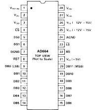 SpecificationsVLL to DGND . . . . . . . . . . . . . . . . . . . . . . ........................ . . . . . 0 V to +7 V
VCC to DGND . . . . . . . . . . . . . . . . . . . . ........................ . . . . . . 0 V to +18 V
VEE to DGND . . . . . . . . . . . . . . . . . . . ...................... . . . . . . . 18 V to 0 V
Soldering . . . . . . . . . . . . . . . . . . . . . ................. . . . . . . . +300°C, 10 sec
Power Dissipation . . . . . . . . . . . . . . . .................... . . . . . . . . . . 1000 mW
AGND to DGND . . . . . . . . . . . . . . . . . . . .......................... . . . . 1 V to +1 V
Reference Input . . . . . VREF ±10 V and VREF (VCC 2 V, VEE + 2 V)
VCC to VEE . . . . . . . . . . . . . . . . . . . . . . .................... . . . . . . . . 0 to +36 V
Digital Inputs . . . . . . . . . . . . . . . . . . . . ..................... . . . . 0.3 V to +7 V
Analog Outputs . . . . . .......... Indefinite Shorts to VCC, VLL, VEE and GNDDescriptionThe AD664 is four complete 12-bit, voltage-output DACs on one monolithic IC chip. Each DAC has a double-buffered input latch structure and a data readback function. All DAC read and write operations occur through a single microprocessor-compatible I/O port.
The I/O port accommodates 4-, 8- or 12-bit parallel words al- lowing simple interfacing with a wide variety of microprocessors.A reset to zero control pin is provided to allow a user to simultaneously reset all DAC outputs to zero, regardless of the contents of the input latch. Any one or all of the DACs may be placed in a transparent mode allowing immediate response by the outputs to the input data.
The analog portion of the AD664 consists of four DAC cells, four output amplifiers, a control amplifier and switches. Each DAC cell is an inverting R-2R type. The output current from each DAC is switched to the on-board application resistors and output amplifier. The output range of each DAC cell is programmedthrough the digital I/O port and may be set to unipolar or bipolar range, with a gain of one or two times the reference voltage. All DACs are operated from a single external reference.
The functional completeness of the AD664 results from the combination of Analog Devices' BiMOS II process, laser-trimmed thin-film resistors and double-level metal interconnects.

 AD664 Data Sheet