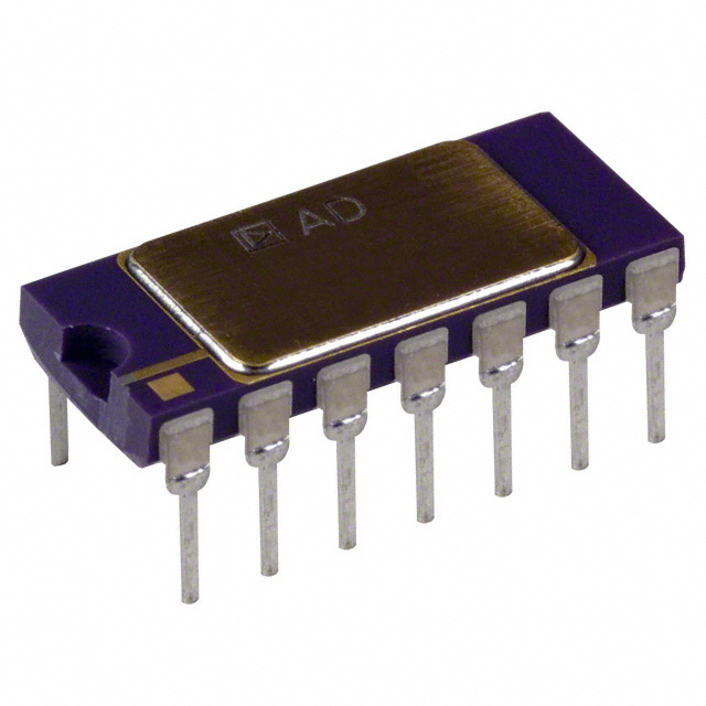
Series: -
Mounting Type: Through Hole
Packaging: Tube
Manufacturer: Analog Devices Inc
Type: Voltage to Frequency
Full Scale: ±50ppm/°C
Package / Case: 8-DIP (0.300", 7.62mm)
Supplier Device Package: 8-PDIP
Frequency - Max: 500kHz
Linearity: ±0.2%
DescriptionThe AD654JN is one member of the AD654 series.The AD654 is a monolithic V/F converter consisting of an input amplifier, a precision oscillator system, and a high current output stage. A single RC network is all that is required to set up any full scale (FS) frequency up to 500 kHz and any FS input voltage up to ± 30 V. Linearity error is only 0.03% for a 250 kHz FS,and operation is guaranteed over an 80 dB dynamic range.
Features of the AD654JN are:(1)low cost; (2)single or dual supply, 5 V to 36 V, 65 V to 618 V; (3)full-scale frequency Up to 500 kHz; (4)minimum number of external components needed; (5)versatile input amplifier:positive or negative voltage modes,negative current mode,high input impedance, low drift; (6)low power: 2.0 mA quiescent current; (7)low offset: 1 mV.Packaged in both an 8-lead mini-DIP and an 8-lead SOIC package, the AD654 is a complete V/F converter requiring only an RC timing network to set the desired full-scale frequency and a selectable pull-up resistor for the open-collector output stage. Any full scale input voltage range from 100 mV to 10 volts (or greater, depending on +VS) can be accommodated by proper selection of the timing resistor.
The absolute maximum ratings of the AD654JN can be summarized as:(1)total supply voltage:36V;(2)storage temperature:-65 to +150;(3)maximum input voltage(pins 3, 4) to VS:300 mV to +VS;(4)maximum output current instantaneous:50 mA;(5)logic common to VS:500 mV to (+VS 4).The AD654's block diagram appears in Figure 1. A versatile operational amplifier serves as the input stage; its purpose is to convert and scale the input voltage signal to a drive current in the NPN follower. Optimum performance is achieved when, at the full-scale input voltage, a 1 mA drive current is delivered to the current-to-frequency converter (an astable multivibrator). The drive current provides both the bias levels and the charging current to the externally connected timing capacitor. This "adaptive" bias scheme allows the oscillator to provide low nonlinearity over the entire current input range of 100 nA to 2 mA. The square wave oscillator output goes to the output driver which provides a floating base drive to the NPN power transistor.
Parameters: | Technical/Catalog Information | AD654JN |
| Vendor | Analog Devices Inc |
| Category | Integrated Circuits (ICs) |
| Package / Case | 8-DIP (300 mil) |
| Type | Voltage to Frequency |
| Frequency-Max | 500kHz |
| Linearity | ±0.2% |
| Full Scale | ±50ppm/°C |
| Packaging | Tube |
| RoHS Status | RoHS Non-Compliant |
| Other Names | AD654JN
AD654JN
|

 AD654JN Data Sheet


