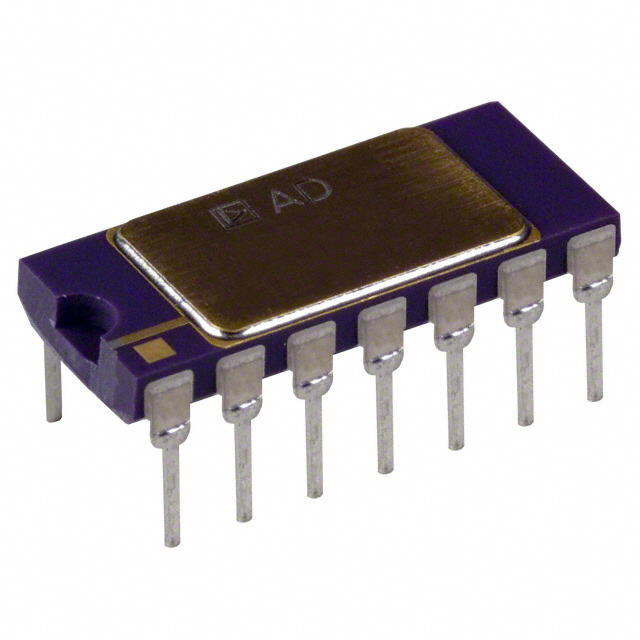
DescriptionThe AD650SD/883B is one member of the AD650 series.The AD650 V/F/V (voltage-to-frequency or frequency-to-voltage converter) provides a combination of high frequency operation and low nonlinearity previously unavailable in monolithic form.The inherent monotonicity of the V/F transfer function makes the AD650 useful as a high-resolution analog-to-digital converter.A flexible input configuration allows a wide variety of input voltage and current formats to be used, and an open-collector output with separate digital ground allows simple interfacing to either standard logic families or opto-couplers.
Features of the AD650SD/883B are:(1)V/F conversion to 1 MHz; (2)reliable monolithic construction; (3)very low nonlinearity:0.002% typ at 10 kHz,0.005% typ at 100 kHz,0.07% typ at 1 MHz; (4)input offset trimmable to zero; (5)CMOS or TTL compatible; (6)unipolar, bipolar, or differential V/F; (7)V/F or F/V conversion; (8)available in surface mount; (9)MIL-STD-883 compliant versions available.In addition to analog-to-digital conversion, the AD650 can be used in isolated analog signal transmission applications, phased lockedloop circuits, and precision stepper motor speed controllers. In the F/V mode, the AD650 can be used in precision tachometer and FM demodulator circuits.
The absolute maximum ratings of the AD650SD/883B can be summarized as:(1)total supply voltage:36V;(2)storage temperature:-55 to +150;(3)differential input voltage:±10 V;(4)maximum input voltage:±VS;(5)open collector output voltage above digital GND:36V;(6)amplifier short circuit to ground:indefinite.The AD650 is a charge balance voltage-to-frequency converter. In the connection diagram shown in Figure 1, or the block diagram of Figure 2a, the input signal is converted into an equivalent current by the input resistance RIN. This current is exactly balanced by an internal feedback current delivered in short, timed bursts from the switched 1 mA internal current source. These bursts of current may be thought of as precisely defined packets of charge.The required number of charge packets, each producing one pulse of the output transistor, depends upon the amplitude of the input signal. Since the number of charge packets delivered per unit time is dependent on the input signal amplitude, a linear voltage-to-frequency transformation will be accomplished. The frequency output is furnished via an open collector transistor.

 AD650SD/883B Data Sheet


