AD566AJD

Features: Single Chip Construction Very High-Speed Settling to 1/2 LSB AD565A: 250 ns max AD566A: 350 ns max Full-Scale Switching Time: 30 ns Guaranteed for Operation with ± 12 V Supplies: AD565A with 12 V Supply: AD566A Linearity Guaranteed Over Temperature: 1/2 LSB max (K, T Grades) Monotonic...

product image

AD566AJD Picture
SeekIC No. : 004269460 Detail

AD566AJD: Features: Single Chip Construction Very High-Speed Settling to 1/2 LSB AD565A: 250 ns max AD566A: 350 ns max Full-Scale Switching Time: 30 ns Guaranteed for Operation with ± 12 V Supplies: AD565A...

floor Price/Ceiling Price

Part Number:
AD566AJD
Supply Ability:
5000

Price Break

  • Qty
  • 1~5000
  • Unit Price
  • Negotiable
  • Processing time
  • 15 Days
Total Cost: $ 0.00

SeekIC Buyer Protection PLUS - newly updated for 2013!

  • Escrow Protection.
  • Guaranteed refunds.
  • Secure payments.
  • Learn more >>

Month Sales

268 Transactions

Rating

evaluate  (4.8 stars)

Upload time: 2025/1/2

Payment Methods

All payment methods are secure and covered by SeekIC Buyer Protection PLUS.

Notice: When you place an order, your payment is made to SeekIC and not to your seller. SeekIC only pays the seller after confirming you have received your order. We will also never share your payment details with your seller.
Product Details

Description


Features:

  Single Chip Construction
  Very High-Speed Settling to 1/2 LSB
       AD565A: 250 ns max
       AD566A: 350 ns max
  Full-Scale Switching Time: 30 ns
  Guaranteed for Operation with ± 12 V Supplies:
      AD565A with 12 V Supply: AD566A
  Linearity Guaranteed Over Temperature:
      1/2 LSB max (K, T Grades)
  Monotonicity Guaranteed Over Temperature
  Low Power:AD566A = 180 mW max;
                        AD565A = 225 mW max
  Use with On-Board High-Stability Reference (AD565A)
     or with External Reference (AD566A)
  Low Cost
  MlL-STD-883-Compliant Versions Available


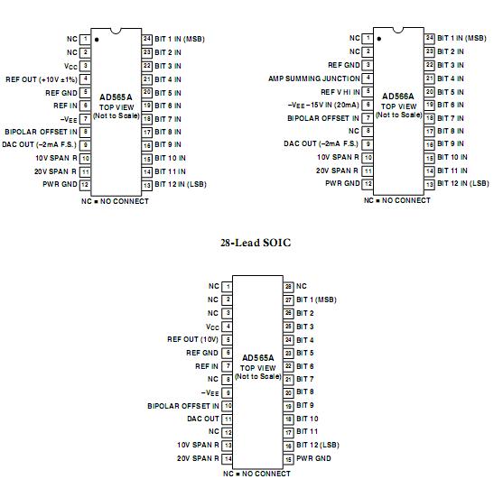
Pinout

  Connection Diagram


Specifications

VCC to Power Ground . . . . . . . . . . . . . . . . . . . . . 0 V to +18 V
VEE to Power Ground (AD565A) . . . . . . . . . . ..    0 V to 18 V
Voltage on DAC Output (Pin 9) . . . . . . . . . . . .  3 V to +12 V
Digital Inputs (Pins 13 to 24) to
  Power Ground . . . . . . . . . . . . . . . . . . . . .    1.0 V to +7.0 V
REF IN to Reference Ground . . . . . . . . . . . . . .   . . . . . . ±12 V
Bipolar Offset to Reference Ground . . . . . . . . . . . .  . . . ±12 V
10 V Span R to Reference Ground . . . . . . . . . . . . . . .   . ±12 V
20 V Span R to Reference Ground . . . . . . . . . . . . .   . . . ±24 V
REF OUT (AD565A) . . . . . ..Indefinite Short to Power Ground
                                                         Momentary Short to VCC
Power Dissipation . . . . . . . . . . . . . . . . . . . . . . . . . . 1000 mW


Description

The AD565A and AD566A are fast 12-bit digital-to-analog converters that incorporate the latest advances in analog circuit design to achieve high speeds at low cost.

The AD565A and AD566A use 12 precision, high-speed bipolar current-steering switches, control amplifier and a laser-trimmed thin-film resistor network to produce a very fast, high accuracy analog output current. The AD565A also includes a buried Zener reference that features low-noise, long-term stability and temperature drift characteristics comparable to the best discrete reference diodes.

The combination of performance and flexibility in the AD565A and AD566A has resulted from major innovations in circuit design, an important new high-speed bipolar process, and continuing advances in laser-wafer-trimming techniques (LWT).

The AD565A and AD566A have a 1090% full-scale transition time less than 35 ns and settle to within ±1/2 LSB in 250 ns max (350 ns for AD566A). Both are laser-trimmed at the wafer level to ±1/8 LSB typical linearity and are specified to ±1/4 LSB max error (K and T grades) at +25°C. High speed and accuracy make the AD565A and AD566A the ideal choice for high-speed display drivers as well as fast analog-to-digital converters.

The laser trimming process which provides the excellent linear- ity is also used to trim both the absolute value and the tempera-ture coefficient of the reference of the AD565A resulting in a typical full-scale gain TC of 10 ppm/°C. When tighter TC performance is required or when a system reference is available, the AD566A may be used with an external reference.


Customers Who Bought This Item Also Bought

Margin,quality,low-cost products with low minimum orders. Secure your online payments with SeekIC Buyer Protection.
Memory Cards, Modules
Optical Inspection Equipment
RF and RFID
Audio Products
Boxes, Enclosures, Racks
View more