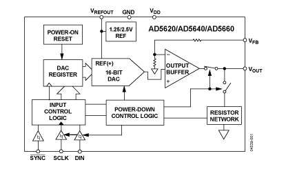
Features: Low power single 16-bit nanoDAC12-bit accuracy guaranteedOn-chip 1.25/2.5 V, 10 ppm/°c referenceTiny 8-lead SOT-23/MSOP packagePower-down to 200 nA @ 5 V, 50 nA @ 3 V3 V/5 V single power supplyGuaranteed 16-bit monotonic by designPower-on-reset to zero/midscaleThree power-down functionsS...
AD5660: Features: Low power single 16-bit nanoDAC12-bit accuracy guaranteedOn-chip 1.25/2.5 V, 10 ppm/°c referenceTiny 8-lead SOT-23/MSOP packagePower-down to 200 nA @ 5 V, 50 nA @ 3 V3 V/5 V single power s...
SeekIC Buyer Protection PLUS - newly updated for 2013!
268 Transactions
All payment methods are secure and covered by SeekIC Buyer Protection PLUS.
Pin No. | Mnemonic | Description |
1 | VDD | Power Supply Input. These parts can operate from 2.7 V to 5.5 V. VDD should be decoupled to GND |
2 | VREFOUT | Reference Voltage Output. |
3 | VFB | Feedback Connection for the output amplifier. VFB should be connected to VOUT for normal operation. |
4 | VOUT | Analog Output Voltage from DAC. The output amplifier has rail-to-rail operation. |
5 | SYNC | Level-Triggered Control Input (Active Low). This is the frame synchronization signal for the input data. When SYNC goes low, it enables the input shift register and data is transferred in on the falling edges of the following clocks. The DAC is updated following the 24th clock cycle for the AD5660 and the 16th clock cycle for AD5620/AD5640 unless SYNC is taken high before this edge. In this case, the rising edge of SYNC acts as an interrupt, and the write sequence is ignored by the DAC. |
6 | SCLK | Serial Clock Input. Data is clocked into the input shift register on the falling edge of the serial clock input. Data can be transferred at rates up to 30 MHz. |
7 | DIN | Serial Data Input. The AD5660 has a 24-bit shift register, and the AD5620/AD5640 have a 16 -bit shift register. Data is clocked into the register on the falling edge of the serial clock input. |
8 | GND | Ground Reference Point for all circuitry on the part. |
Resolution (Bits) | 16bit |
DAC Update Rate | 125kSPS |
DAC Settling Time | 8s |
# DAC Outputs | 1 |
DAC Type | Voltage Out |
DAC Input Format | Ser,SPI |
Output FSR | (Uni 2.5V),(Uni 5V) |
Ref Int/Ext | Int |
Supply Vnom | Single(+2.7 to +5.5),Single(+3),Single(+3.3),Single(+5) |
Pwr Diss | 5mW |
Package | SOP,SOT |
Parameter | Rating |
VDD to GND | −0.3 V to +7 V |
Digital Input Voltage to GND | −0.3 V to VDD + 0.3 V |
VOUT to GND | −0.3 V to VDD + 0.3 V |
Operating Temperature Range Industrial (B Version) | −40°C to +105°C |
Storage Temperature Range | −65°C to +150°C |
Junction Temperature (TJ max) | 150°C |
SOT-23 Package Power Dissipation | (TJ max − TA)/JA |
JA Thermal Impedance | 240°C/W |
Lead Temperature, Soldering Vapor Phase (60 sec) | 215°C |
Infrared (15 sec) | 220°C |