Features: ·Low power, smallest-pin-compatible octal DACs
AD5668: 16 bits
AD5648: 14 bits
AD5628: 12 bits
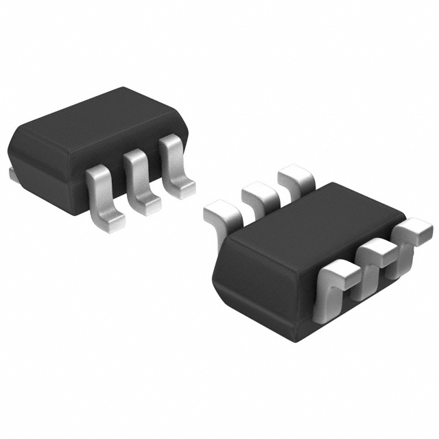
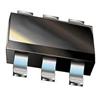
·14-lead/16-lead TSSOP
·On-chip 1.25 V/2.5 V, 5 ppm/°C reference
·Power down to 400 nA @ 5 V, 200 nA @ 3 V
·2.7 V to 5.5 V power supply
·Guaranteed monotonic by design
·Power-on reset to zero scale or midscale
·3 power-down functions
·HardwareLDAC andLDAC override function
·CLR function to programmable code
·Rail-to-rail operationApplication·Process control
·Data acquisition systems
·Portable battery-powered instruments
·Digital gain and offset adjustment
·Programmable voltage and current sources
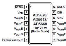
·Programmable attenuatorsPinout
 Specifications
| Resolution (Bits) |
14bit |
| DAC Update Rate |
95kSPS |
| DAC Settling Time |
6s |
| # DAC Outputs |
8 |
| DAC Type |
Voltage Out |
| DAC Input Format |
Ser,SPI |
| Output FSR |
(Uni 2Vref),(Uni Vref) |
| Ref Int/Ext |
Int/Ext |
| Supply Vnom |
Single(+2.7 to +5.5),Single(+2.7),Single(+3),Single(+3.3),Single(+5) |
| Pwr Diss |
2.15mW |
| Package |
SOP |
VDD to GND ...................................................−0.3 V to +7 V
Digital Input Voltage to GND ..............−0.3 V to VDD + 0.3 V
VOUT to GND ......................................−0.3 V to VDD + 0.3 V
VREFIN/VREFOUT to GND...................... −0.3 V to VDD + 0.3 V
Operating Temperature Range
Industrial ...............................................−40°C to +105°C
Storage Temperature Range................. −65°C to +150°C
Junction Temperature (TJ MAX) ...............................+150°C
TSSOP Package
Power Dissipation.................................... (TJ MAX − TA)/JA
JA Thermal Impedance.....................................150.4°C/W
Reflow Soldering Peak Temperature
SnPb......................................................................... 240°C
Pb Free..................................................................... 260°C
Stresses above those listed under Absolute Maximum Ratings may cause permanent damage to the device. This is a stress rating only; functional operation of the device at these or any other conditions above those indicated in the operational section of this specification is not implied. Exposure to absolute maximum rating conditions for extended periods may affect device reliability.
DescriptionAD5628/AD5648/AD5668 devices are low power, octal, 12-/14-/16-bit, buffered voltage-output DACs. All devices operate from a single 2.7 V to 5.5 V supply and are guaranteed monotonic by design.
The AD5628/AD5648/AD5668 devices are low power, octal, 12-/14-/16-bit, buffered voltage-output DACs. All devices operate from a single 2.7 V to 5.5 V supply and are guaranteed monotonic by design.
The AD5628/AD5648/AD5668 have an on-chip reference with an internal gain of 2. The AD5628/AD5648/AD5668-1 have a 1.25 V 5 ppm/°C reference, giving a full-scale output range of 2.5 V; the AD5628/AD5648/AD5668-2, -3 have a 2.5 V 5 ppm/°C reference, giving a full-scale output range of 5 V. The on-board reference is off at power-up, allowing the use of an external reference. The internal reference is enabled via a software write.
The part incorporates a power-on reset circuit that ensures that the DAC output powers up to 0 V (AD5628/AD5648/AD5668-1, -2) or midscale (AD5668-3) and remains powered up at this level until a valid write takes place. The part contains a power-down feature that reduces the current consumption of the device to 400 nA at 5 V and provides software-selectable output loads while in power-down mode for any or all DAC channels.
The outputs of all DACs can be updated simultaneously using theLDAC function, with the added functionality of userselectable DAC channels to simultaneously update. There is also an asynchronousCLR that updates all DACs to a userprogrammable code-zero scale, midscale, or full scale.
The AD5628/AD5648/AD5668 utilize a versatile 3-wire serial interface that operates at clock rates of up to 50 MHz and is compatible with standard SPI®, QSPI™, MICROWIRE™, and DSP interface standards. The on-chip precision output amplifier enables rail-to-rail output swing.

 AD5648 Data Sheet