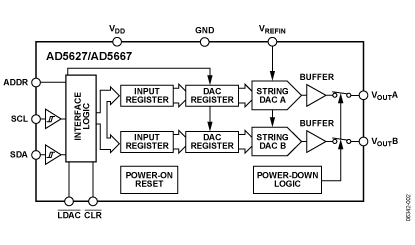
Features: •Low power, smallest pin-compatible, dual nanoDACs•AD5627R/AD5647R/AD5667R 12-/14-/16- bit On-chip 1.25 V/2.5 V, 5 ppm/°C reference•AD5625/AD5665 12-/16- bit External reference only•3 mm x 3 mm LFCSP and 10-lead MSOP•2.7 V to 5.5 V power supply•Guarant...
AD5627: Features: •Low power, smallest pin-compatible, dual nanoDACs•AD5627R/AD5647R/AD5667R 12-/14-/16- bit On-chip 1.25 V/2.5 V, 5 ppm/°C reference•AD5625/AD5665 12-/16- bit External ref...
SeekIC Buyer Protection PLUS - newly updated for 2013!
268 Transactions
All payment methods are secure and covered by SeekIC Buyer Protection PLUS.
Resolution (Bits) | 12bit |
DAC Update Rate | 333kSPS |
DAC Settling Time | 3s |
# DAC Outputs | 2 |
DAC Type | Voltage Out |
DAC Input Format | I2C/Ser 2-wire,Ser |
Output FSR | (Uni Vref) |
Ref Int/Ext | Ext |
Supply Vnom | Single(+2.7 to +5.5),Single(+3),Single(+3.3),Single(+5) |
Pwr Diss | 5.75mW |
Package | CSP,SOP |
Parameter |
Rating |
VDD to GND VOUT to GND VREFIN/VREFOUT to GND Digital Input Voltage to GND Operating Temperature Range Industrial Storage Temperature Range Junction Temperature (TJ max) Power Dissipation LFCSP_WD Package (4-Layer Board) JA Thermal Impedance MSOP Package JA Thermal Impedance Reflow Soldering Peak Temperature Pb-Free |
−0.3 V to +7 V −0.3 V to VDD + 0.3 V −0.3 V to VDD + 0.3 V −0.3 V to VDD + 0.3 V −40°C to +105°C −65°C to +150°C 150°C (TJ max − TA)/JA 61°C/W 150.4°C/W 260°C ± 5°C |
The AD5627R/AD5647R/AD5667R, AD5627/AD5667, members of the nanoDAC family, are low power, dual, 12-, 14-, 16-bit buffered voltage-out DACs with/without on-chip reference. All devices operate from a single 2.7 V to 5.5 V supply, are guaranteed monotonic by design and have an I2Ccompatible serial interface .
The AD5627R/AD5647R/AD5667R have an on-chip reference. The AD56x7RBCPZ have a 1.25 V, 5 ppm/°C reference, giving a full-scale output range of 2.5 V; the AD56x7RBRUZ have a 2.5 V, 5 ppm/°C reference giving a full-scale output range of 5 V. The on-chip reference is off at power-up, allowing the use of an external reference. The internal reference is enabled via a software write. The AD5667 and AD5627 require an external reference voltage to set the output range of the DAC The part incorporates a power-on reset circuit that ensures the DAC output powers up to 0 V and remains there until a valid write takes place.
The part contains a per-channel power-down feature that reduces the current consumption of the device to 480 nA at 5 V and provides software-selectable output loads while in power-down mode. The low power consumption of this part in normal operation makes it ideally suited to portable battery-operated equipment. The on-chip precision output amplifier enables rail-to-rail output swing.
The AD5627R/AD5647R/AD5667R, AD5627/AD5667 use a 2- wire I2C-compatible serial interface that operates in standard (100 kHz), fast (400 kHz), and high speed (3.4 MHz) modes.