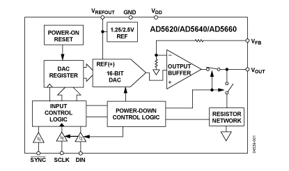
Features: Low power, single nanoDACs
AD5660: 16 bits
AD5640: 14 bits
AD5620: 12 bits
12-bit accuracy guaranteed
On-chip, 1.25 V/2.5 V, 5 ppm/°C reference
Tiny 8-lead SOT-23/MSOP packages
Power-down to 480 nA @ 5 V, 200 nA @ 3 V
3 V/5 V single power supply
Guaranteed 16-bit monotonic by design
Power-on reset to zero/midscale
3 power-down functions
Serial interface with Schmitt-triggered inputs
Rail-to-rail operation
SYNC interrupt facilityApplicationProcess control
Data acquisition systems
Portable battery-powered instruments
Digital gain and offset adjustment
Programmable voltage and current sources
Programmable attenuatorsPinout

| Pin No. |
Mnemonic |
Description |
| 1 |
VDD |
Power Supply Input. These parts can operate from 2.7 V to 5.5 V. VDD should be decoupled to GND |
| 2 |
VREFOUT |
Reference Voltage Output. |
| 3 |
VFB |
Feedback Connection for the output amplifier. VFB should be connected to VOUT for normal operation. |
| 4 |
VOUT |
Analog Output Voltage from DAC. The output amplifier has rail-to-rail operation. |
| 5 |
SYNC |
Level-Triggered Control Input (Active Low). This is the frame synchronization signal for the input data. When SYNC goes low, it enables the input shift register and data is transferred in on the falling edges of the following clocks. The DAC is updated following the 24th clock cycle for the AD5660 and the 16th clock cycle for AD5620/AD5640 unless SYNC is taken high before this edge. In this case, the rising edge of SYNC acts as an interrupt, and the write sequence is ignored by the DAC. |
| 6 |
SCLK |
Serial Clock Input. Data is clocked into the input shift register on the falling edge of the serial clock input. Data can be transferred at rates up to 30 MHz. |
| 7 |
DIN |
Serial Data Input. The AD5660 has a 24-bit shift register, and the AD5620/AD5640 have a 16 -bit shift register. Data is clocked into the register on the falling edge of the serial clock input. |
| 8 |
GND |
Ground Reference Point for all circuitry on the part. |
Specifications
| Resolution (Bits) |
12bit |
| DAC Update Rate |
125kSPS |
| DAC Settling Time |
8s |
| # DAC Outputs |
1 |
| DAC Type |
Voltage Out |
| DAC Input Format |
Ser,SPI |
| Output FSR |
(Uni 2.5V),(Uni 5V) |
| Ref Int/Ext |
Int |
| Supply Vnom |
Single(+2.7 to +5.5),Single(+2.7),Single(+3),Single(+3.3),Single(+5) |
| Pwr Diss |
5mW |
| Package |
SOP,SOT |
| Parameter |
Rating |
| VDD to GND |
−0.3 V to +7 V |
| VOUT to GND |
−0.3 V to VDD + 0.3 V |
| VFB to GND |
−0.3 V to VDD + 0.3 V |
| VREFOUT to GND |
−0.3 V to VDD + 0.3 V |
| Digital Input Voltage to GND |
−0.3 V to VDD + 0.3 V |
|
Operating Temperature Range
Industrial |
−15°C to +105°C |
| Storage Temperature Range |
−65°C to +150°C |
| Junction Temperature (TJ max) |
150°C |
| Power Dissipation |
(TJ max − TA)/JA |
SOT-23 Package (4-Layer Board)
JA Thermal Impedance |
119°C/W |
MSOP Package (4-Layer Board)JA Thermal Impedance 141°C/W
JC Thermal Impedance |
|
| Reflow Soldering Peak Temperature |
|
| SnPb |
|
| Pb-Free |
260°C |
DescriptionThe AD5620/AD5640/AD5660, members of the nanoDAC family of devices, are low power, single, 12-/14-/16-bit, buffered voltage-out DACs and are guaranteed monotonic by design.
The AD5620/AD5640/AD5660-1 parts include an internal, 1.25 V, 5 ppm/°C reference, giving a full-scale output voltage range of 2.5 V. The AD5620/AD5640/AD5660-2-3 parts include an internal, 2.5 V, 5 ppm/°C reference, giving a full-scale output voltage range of 5 V. The reference associated with each part is available at the VREFOUT pin.
The parts incorporate a power-on reset circuit to ensure that the DAC output powers up to 0 V (AD5620/AD5640/AD5660-1-2) or midscale (AD5620-3 and AD5660-3) and remains there until a valid write takes place. The parts contain a power-down feature that reduces the current consumption of the device to 480 nA at 5 V and provides software-selectable output loads while in power-down mode. The power consumption is 2.5 mW at 5 V, reducing to 1 W in power-down mode.
The AD5620/AD5640/AD5660 on-chip precision output amplifier allows rail-to-rail output swing to be achieved. For remote sensing applications, the output amplifier's inverting input is available to the user. The AD5620/AD5640/AD5660 use a versatile 3-wire serial interface that operates at clock rates up to 30 MHz and is compatible with standard SPI®, QSPI™, MICROWIRE™, and DSP interface standards.

 AD5620 Data Sheet


