Features: `12-Bit Linearity and Monotonic 40 to +125`Single +5V to +12V or dual ±5V supply`Unipolar or Bipolar Operation`Double Buffered Registers Enable Simultaneous Multi- Channels Update`4 Separate Rail-to Rail Reference Inputs`Parallel Interface`Data Readback Capability`5s Settling TimeApplica...
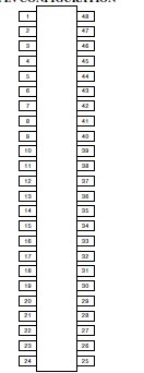
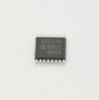
AD5583: Features: `12-Bit Linearity and Monotonic 40 to +125`Single +5V to +12V or dual ±5V supply`Unipolar or Bipolar Operation`Double Buffered Registers Enable Simultaneous Multi- Channels Update`4 Separa...
SeekIC Buyer Protection PLUS - newly updated for 2013!
268 Transactions
All payment methods are secure and covered by SeekIC Buyer Protection PLUS.
VDD to VSS.......................................................-0.3V to +16.5V
VDD to GND.......................................................... -0.3V to 5.5V
VSS to GND.........................................................+0.3V to -5.5V
VDD to VREF+............................................. -0.3V to (VDD-VSS)
VREF- to VSS............................................... -0.3V to (VDD-VSS)
VREFH to VREFL ........................................ -0.3V to (VDD-VSS)
Logic Inputs to GND............................VSS 0.3V, VDD + 0.3V
VOUT to GND.......................................VSS 0.3V, VDD + 0.3V
IOUT Short Circuit to GND.........................................................
Thermal Resistance JA
TSSOP-48 Lead (RU-48) ........................................... xxx°C/W
Maximum Junction Temperature (TJ MAX) .................... 150°C
Package Power Dissipation = (TJ MAX TA)/J
Operating Temperature Range ................40°C to +125°C
Storage Temperature Range ...................65°C to +150°C
Lead Temperature:
RU-48 (Vapor Phase, 60 secs)...................................... xxx°C
RU-44 (Infrared, 15 secs) ............................................ xxx°C
Stress above those listed under "Absolute Maximum Ratings" may cause permanent damage to the device. This is a stress rating only and functional operation of the device at these or any other conditions above those indicated in the operational sections of this specification is not implied. Exposure to absolute maximum rating conditions for extended periods may affect device reliability.
The AD5582/AD5583 family of quad, 12-/10-bit, voltage-output digital-to-analog converter is designed to operate from a single +5 to +15 volt or a dual ±5V supply. Built using a CBCMOS process, this monolithic DAC offers the user low cost, and ease-of-use in single or dual-supply systems.
The applied external reference VREF determines the full-scale output voltage. Valid VREF values include VSS<VREF<VDD resulting in a wide selection of full scale outputs. For multiplying applications AC inputs can be as large as |VDD-VSS|. Two on-board precision trimmed resistors are available for 4-Quadrant configurations.
A doubled-buffered parallel interface offers 25Mbps data load rates. A common level-sensitive load-DAC strobe (LDAC) input allows simultaneous update of all DAC outputs from previously loaded Input Registers. An external asynchronous reset (LDAC) forces all registers to the zero code state when MSB='0' or to midscale when MSB='1'.
Both parts are offered in the same pin-out to allow users to select the amount of resolution appropriate for their application without circuit card redesign.
The AD5582/AD5583 are specified over the extended industrial (-40°C to +125°C) temperature range. Packages available include thin 1.1 mm TSSOP-48 package.