AD5532HS

Features: `High Integration: 32-Channel DAC in 12*12 mm2 LFBGA`Guaranteed Monotonic`DSP-/Microcontroller-Compatible Serial Interface`Channel Update Rate 1.1 MHz`Output Impedance 0.5`Selectable Output Voltage 0 V to 5 V or 2.5 V to +2.5 V`AsynchronousRESET Facility`Temperature Range 40C to +85CAp...

product image

AD5532HS Picture
SeekIC No. : 004269368 Detail

AD5532HS: Features: `High Integration: 32-Channel DAC in 12*12 mm2 LFBGA`Guaranteed Monotonic`DSP-/Microcontroller-Compatible Serial Interface`Channel Update Rate 1.1 MHz`Output Impedance 0.5`Selectable Outpu...

floor Price/Ceiling Price

Part Number:
AD5532HS
Supply Ability:
5000

Price Break

  • Qty
  • 1~5000
  • Unit Price
  • Negotiable
  • Processing time
  • 15 Days
Total Cost: $ 0.00

SeekIC Buyer Protection PLUS - newly updated for 2013!

  • Escrow Protection.
  • Guaranteed refunds.
  • Secure payments.
  • Learn more >>

Month Sales

268 Transactions

Rating

evaluate  (4.8 stars)

Upload time: 2024/12/21

Payment Methods

All payment methods are secure and covered by SeekIC Buyer Protection PLUS.

Notice: When you place an order, your payment is made to SeekIC and not to your seller. SeekIC only pays the seller after confirming you have received your order. We will also never share your payment details with your seller.
Product Details

Description


Features:

`High Integration: 32-Channel DAC in 12*12 mm2 LFBGA
`Guaranteed Monotonic
`DSP-/Microcontroller-Compatible Serial Interface
`Channel Update Rate 1.1 MHz
`Output Impedance 0.5
`Selectable Output Voltage 0 V to 5 V or 2.5 V to +2.5 V
`Asynchronous RESET Facility
`Temperature Range 40C to +85C


Application

·Optical Networks
·Level Setting
·Instrumentation
·Automatic Test Equipment
·Industrial Control Systems
·Data Acquisition
·Low Cost I/O


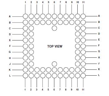
Pinout

  Connection Diagram


Specifications

VDD to AGND . . . . . . . . . . . . . . . . . . . . . . .  0.3 V to +17 V
VSS to AGND . . . . . . . . . . . . . . . . . . . . . . ... +0.3 V to 17 V
AVCC to AGND, DAC_GND . . . . . . . . . . . .. .....0.3 V to +7 V
DVCC to DGND . . . . . . . . . . . . . . . . . . . .. . . ..0.3 V to +7 V
Digital Inputs to DGND . . . . . . . . . .. 0.3 V to DVCC + 0.3 V
REF_IN to AGND, DAC_GND . . . . . . . . .. . . ....0.3 V to +7 V
VOUT0VOUT31 to AGND . . . . ...  VSS 0.3 V to VDD + 0.3 V
VOUT0VOUT31 to VSS . . . . . . . . . .. . . . . . .0.3 V to +24 V
OFFS_IN to AGND . . . . . . . . . . . .VSS 0.3 V to VDD + 0.3 V
AGND to DGND . . . . . . . . . . . . . . . . . . . . .. 0.3 V to +0.3 V
Operating Temperature Range
Industrial . . . . . . . . . . . . . . . . . . . . . . . . .  40°C to +85°C
Storage Temperature Range . . . . . . . . .  65°C to +150°C
Junction Temperature (TJ max) . . . . . . . . . . . . . . . . . 150°C
74-Lead LFBGA Package, JA Thermal Impedance . .41°C/W
Reflow Soldering
Peak Temperature . . . . . . . . . . . . . . . . . . . . . . . . . . 220°C
Time at Peak Temperature . . . . . . . . . . . . 10 sec to 40 sec
Max Power Dissipation at TA = 70°C,
Outputs Loaded . . . . . . . . . . . . . . . . . . . . . . . . . . 550 mW3
(for TA > 70°C, derate at 26 mW for each °C over 70°C)

NOTES
1 Stresses above those listed under Absolute Maximum Ratings may cause permanent damage to the device. This is a stress rating only; functional operation of the device at these or any other conditions above those listed in the operational sections of this specification is not implied. Exposure to absolute maximum rating conditions for extended periods may affect device reliability.
2 Transient currents of up to 100 mA will not cause SCR latch-up.
3 This limit includes load power and applies only when there is a resistive load on VOUT outputs.


Description

The AD5532HS is a 32-channel voltage-output 14-bit DAC with a high-speed serial interface. The selected DAC register is written to via the 3-wire interface. The serial interface operates at clock rates up to 30 MHz and is compatible with DSP and microcontroller interface standards. The output voltage range is 0 V to 5 V or 2.5 V to +2.5 V and is determined by the offset voltage at the OFFS_IN pin. It is restricted to a range from VSS + 2 V to VDD 2 V because of the headroom of the output amplifier.

The device AD5532HS is operated with AVCC = 5 V ± 5%, DVCC = 2.7 V to 5.25 V, VSS = 4.75 V to 12 V and VDD = +4.75 V to +12 V and requires a stable 2.5 V reference on REF_IN.


Customers Who Bought This Item Also Bought

Margin,quality,low-cost products with low minimum orders. Secure your online payments with SeekIC Buyer Protection.
Motors, Solenoids, Driver Boards/Modules
LED Products
Test Equipment
Static Control, ESD, Clean Room Products
Prototyping Products
DE1
View more