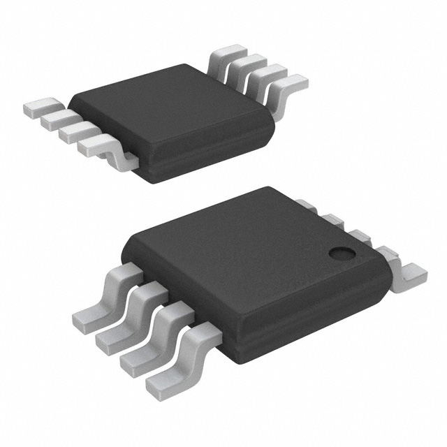
Features: 40-channel DAC in 13 mm × 13 mm 108-lead CSPBGA
Guaranteed monotonic to 14 bits
Buffered voltage outputs Output
voltage span of 3.5 V × VREF(+)
Maximum output voltage span of 17.5 V
System calibration function allowing user-programmable offset and gain
Pseudo differential outputs relative to REFGND
Clear function to user-defined REFGND (CLR pin)
Simultaneous update of DAC outputs (LDAC pin)
DAC increment/decrement mode
Channel grouping and addressing features Interface options:
Parallel interface
DSP/microcontroller-compatible 3-wire serial interface
2.5 V to 5.5 V JEDEC-compliant digital levels
SDO daisy-chaining option
Power-on reset
Digital reset (RESET pin and soft reset function)ApplicationLevel setting in automatic test equipment (ATE)
Variable optical attenuators (VOA)
Optical switches
Industrial control systemsPinout SpecificationsParameter Rating
VDD to AGND −0.3 V to +17 V
VSS to AGND −17 V to +0.3 V
VCC to DGND −0.3 V to +7 V
Digital Inputs to DGND −0.3 V to VCC + 0.3 V
Digital Outputs to DGND −0.3 V to VCC + 0.3 V
VREF1(+), VREF2(+) to AGND −0.3 V to +7 V
VREF1(−), VREF2(−) to AGND VSS − 0.3 V to VDD + 0.3 V
VBIAS to AGND −0.3 V to +7 V
VOUT0VOUT39 to AGND VSS − 0.3 V to VDD + 0.3 V
REFGND to AGND VSS − 0.3 V to VDD + 0.3 V
AGND to DGND −0.3 V to +0.3 V
Operating Temperature Range (TA)
Industrial (A Version) −40°C to +85°C
Storage Temperature Range −65°C to +150°C
Junction Temperature (TJ max) 150°C
108-Lead CSPBGA Package
JA Thermal Impedance 37.5°C/W
JC Thermal Impedance 8.5°C/W
Reflow Soldering
Peak Temperature 230°C
Time at Peak Temperature 10 s to 40 sDescriptionThe AD5379 contains 40, 14-bit DACs in one CSPBGA package.The AD5379 provides a bipolar output range determined by the voltages applied to the VREF(+) and VREF(−) inputs. The maximum output voltage span is 17.5 V, corresponding to a bipolar output range of −8.75 V to +8.75 V, and is achieved with reference voltages of VREF(−) = −3.5 V and VREF(+) = +5 V.
The AD5379 offers guaranteed operation over a wide VSS/VDD supply range from ±11.4 V to ±16.5 V. The output amplifier headroom requirement is 2.5 V operating with a load current of 1.5 mA and 2 V operating with a load current of 0.5 mA.
The AD5379 contains a double-buffered parallel interface in which 14 data bits are loaded into one of the input registers under thecontrol of the WR, CS, and DAC channel address pins, A0 to A7. It also has a 3-wire serial interface, which is compatible with SPI®, QSPI™, MICROWIRE™, and DSP interface standards and can handle clock speeds of up to 50 MHz.
The DAC outputs are updated on reception of new data into the DAC registers. All the outputs can be updated simultaneously by taking the LDAC input low. Each channel has a programmable gain and an offset adjust register.
Each DAC output is gained and buffered on-chip with respect to an external REFGND input. The DAC outputs can also be switched to REFGND via the CLR pin.

 AD5379 Data Sheet


