AD5373

Features: ·32-channel DAC in 56-LFCSP and 64-LQFP·AD5372 Guaranteed monotonic to 16 bits·AD5373 Guaranteed monotonic to 14 bits·Maximum output voltage span of 4 × VREF (20 V)·Nominal output voltage range of -4 V to +8 V·Multiple, independent output spans available·System calibration function allow...

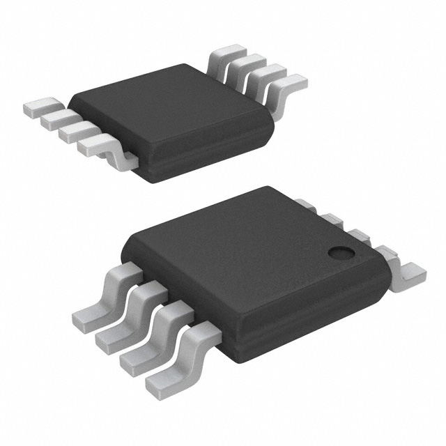
product image

AD5373 Picture
SeekIC No. : 004269215 Detail

AD5373: Features: ·32-channel DAC in 56-LFCSP and 64-LQFP·AD5372 Guaranteed monotonic to 16 bits·AD5373 Guaranteed monotonic to 14 bits·Maximum output voltage span of 4 × VREF (20 V)·Nominal output voltage ...

floor Price/Ceiling Price

Part Number:
AD5373
Supply Ability:
5000

Price Break

  • Qty
  • 1~5000
  • Unit Price
  • Negotiable
  • Processing time
  • 15 Days
Total Cost: $ 0.00

SeekIC Buyer Protection PLUS - newly updated for 2013!

  • Escrow Protection.
  • Guaranteed refunds.
  • Secure payments.
  • Learn more >>

Month Sales

268 Transactions

Rating

evaluate  (4.8 stars)

Upload time: 2024/11/9

Payment Methods

All payment methods are secure and covered by SeekIC Buyer Protection PLUS.

Notice: When you place an order, your payment is made to SeekIC and not to your seller. SeekIC only pays the seller after confirming you have received your order. We will also never share your payment details with your seller.
Product Details

Description


Features:

·32-channel DAC in 56-LFCSP and 64-LQFP
·AD5372 Guaranteed monotonic to 16 bits
·AD5373 Guaranteed monotonic to 14 bits
·Maximum output voltage span of 4 × VREF (20 V)
·Nominal output voltage range of -4 V to +8 V
·Multiple, independent output spans available
·System calibration function allowing user-programmable offset and gain
·Channel grouping and addressing features
·Thermal Monitoring Function
·DSP/microcontroller-compatible serial interface
·2.5 V to 5.5 V JEDEC-compliant digital levels
·Power-on reset
·Digital reset (RESET)
·Clear function to user-defined SIGGND (CLR pin)
·Simultaneous update of DAC outputs (LDAC pin)


Application

·Level setting in automatic test equipment (ATE)
·Variable optical attenuators (VOA)
·Optical switches
·Industrial control systems
·Instrumentation


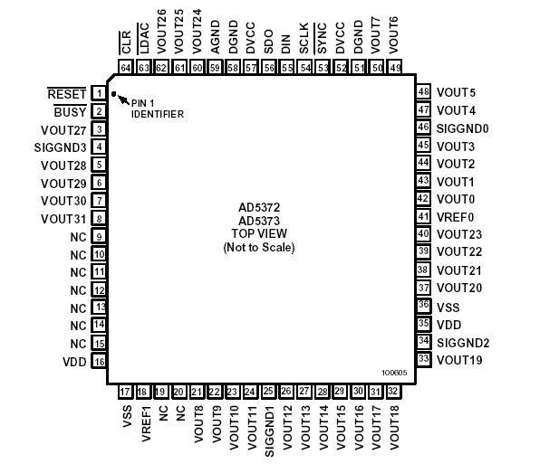
Pinout

  Connection Diagram

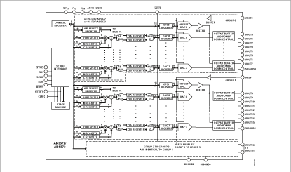
AD5373 Diagram


Specifications

Parameter
Rating
VDD to AGND
VSS to AGND
DVCC to DGND
Digital Inputs to DGND
Digital Outputs to DGND
VREF1, VREF2 to AGND
VOUT0VOUT39 to AGND
SIGGND to AGND
AGND to DGND
Operating Temperature Range (TA)
Industrial (B Version)
Storage Temperature Range
Junction Temperature (TJ max)
JA Thermal Impedance
56-LFCSP
64-LQFP
Reflow Soldering
Peak Temperature
Time at Peak Temperature
−0.3 V to +17 V
−17 V to +0.3 V
−0.3 V to +7 V
−0.3 V to VCC + 0.3 V
−0.3 V to +7 V
VSS − 0.3 V to VDD + 0.3 V
−0.3 V to +0.3 V

−40°C to +85°C
−65°C to +150°C
130°C

24°C/w
45.5°C/w

230°C
10 s to 40 s


DAC Input Format Ser,SPI
# DAC Outputs 32
Pwr Diss 520mW
DAC Uni or Bip Uni/Bip
DAC Vout Swing max 20V p-p
Output FSR (Bip 2Vref),(Uni 4 x VRef)
Package QFP
Resolution (Bits) 14bit
Supply Vnom Multi(±15, +2.5Dig) ,Multi(±15, +3.3Dig) ,Multi(±15, +3Dig),Multi(±15, +5Dig)


Description

The AD5372 and AD5373 contain 32, 16-bit or 14-bit DACs in a single, 56-lead, LFCSP or 64-lead LQFP package. The AD5372/AD5373 provides buffered voltage outputs with a span 4 times the reference voltage. The gain and offset of each DAC can be independently trimmed to remove errors. For even greater flexibility, the device is divided into 4 groups of 8 DACs. Two offset DACs allow the output range of the groups to be altered.

The ADAD5372/AD5373 offers guaranteed operation over a wide supply range with VSS from -4.5 V to -16.5 V and VDD from+8 V to +16.5 V. The output amplifier headroom requirement is 1.4 V operating with a load current of 1 mA.

The ADAD5372/AD5373 has a high-speed serial interface, which is compatible with SPI®, QSPI™, MICROWIRE™, and DSP interface standards and can handle clock speeds of up to 50 MHz.

The DAC outputs are updated on reception of new data into the DAC registers. All the outputs can be updated simultaneously by taking the LDAC input low. Each channel has a programmable gain and an offset adjust register.

Each DAC output is gained and buffered on-chip with respect to an external SIGGND input. The DAC outputs can also be switched to SIGGND via theCLR pin.


Customers Who Bought This Item Also Bought

Margin,quality,low-cost products with low minimum orders. Secure your online payments with SeekIC Buyer Protection.
Undefined Category
Test Equipment
Sensors, Transducers
Hardware, Fasteners, Accessories
Fans, Thermal Management
Integrated Circuits (ICs)
View more