AD5348*

Features: ` AD5346: Octal 8-Bit DAC` AD5347: Octal 10-Bit DAC` AD5348: Octal 12-Bit DAC` Low Power Operation: 1.4 mA (max) @ 3 V` Power-Down to 100 nA @ 3 V, 240 nA @ 5 V` Guaranteed Monotonic by Design Over All Codes` Rail-to-Rail Output Range: 0VREF or 02 VREF` Power-On Reset to Zero Volts` Simu...

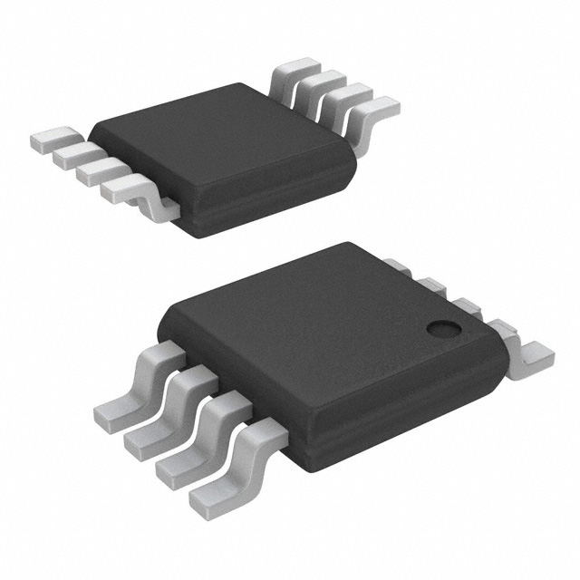
product image

AD5348* Picture
SeekIC No. : 004269180 Detail

AD5348*: Features: ` AD5346: Octal 8-Bit DAC` AD5347: Octal 10-Bit DAC` AD5348: Octal 12-Bit DAC` Low Power Operation: 1.4 mA (max) @ 3 V` Power-Down to 100 nA @ 3 V, 240 nA @ 5 V` Guaranteed Monotonic by De...

floor Price/Ceiling Price

Part Number:
AD5348*
Supply Ability:
5000

Price Break

  • Qty
  • 1~5000
  • Unit Price
  • Negotiable
  • Processing time
  • 15 Days
Total Cost: $ 0.00

SeekIC Buyer Protection PLUS - newly updated for 2013!

  • Escrow Protection.
  • Guaranteed refunds.
  • Secure payments.
  • Learn more >>

Month Sales

268 Transactions

Rating

evaluate  (4.8 stars)

Upload time: 2024/6/7

Payment Methods

All payment methods are secure and covered by SeekIC Buyer Protection PLUS.

Notice: When you place an order, your payment is made to SeekIC and not to your seller. SeekIC only pays the seller after confirming you have received your order. We will also never share your payment details with your seller.
Product Details

Description


Features:

` AD5346: Octal 8-Bit DAC
` AD5347: Octal 10-Bit DAC
` AD5348: Octal 12-Bit DAC
` Low Power Operation: 1.4 mA (max) @ 3 V
` Power-Down to 100 nA @ 3 V, 240 nA @ 5 V
` Guaranteed Monotonic by Design Over All Codes
` Rail-to-Rail Output Range: 0VREF or 02 VREF
` Power-On Reset to Zero Volts
` Simultaneous Update of DAC Outputs via LDAC Pin
` Asynchronous CLR Facility
` Readback
` Buffered/Unbuffered Reference Inputs
` 20ns WR time
` 3`8-lead TSSOP/6mm x 6mm 40-lead CSP Packaging
` Temperature Range: 40C to +105C


Application

· Portable Battery-Powered Instruments
· Digital Gain and Offset Adjustment
· Programmable Voltage and Current Sources
· Optical Networking
· Automatic Test Equipment
· Mobile Communications
· Programmable Attenuators
· Industrial Process Control


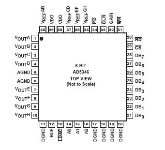
Pinout

  Connection Diagram


Specifications

VDD to GND . . . . . . . . . . . . . . . . . . . . . . . . 0.3 V to +7 V
Digital Input Voltage to GND . . . .  . 0.3 V to VDD + 0.3 V
Digital Output Voltage to GND . . .  ..0.3 V to VDD + 0.3 V
Reference Input Voltage to GND  . . 0.3 V to VDD + 0.3 V
VOUT to GND . . . . . . . . . . . . . . . . . .0.3 V to VDD + 0.3 V
Operating Temperature Range
Industrial (B Version) . . . . . . . . . . . . . . 40°C to +105°C
Storage Temperature Range . . . . . . . . .65°C to +150°C
Junction Temperature . . . . . . . . . . . . . . . . . . . . . . .150°C
38-lead TSSOP Package
Power Dissipation . . . . . . . . . . .  . . (TJ max TA)/JA mW
JA Thermal Impedance . . . . . . . . . . . . . . . . . . 98.3°C/W
JC Thermal Impedance . . . . . . . . . . . . . . . . . . . 8.9°C/W
40-lead CSP Package
Power Dissipation . . . . . . . . . . . .  . (TJ max TA)/JA mW
JA Thermal Impedance . . . . . . . . . . . . . . . . . . .  30°C/W
JC Thermal Impedance . . . . . . . . . . . . . . . . . . . . .  °C/W
Lead Temperature, Soldering (10 seconds) . . . . . . 300°C
IR Reflow, Peak Temperature . . . . . . . . . . . . . . .  +220°C
*Stresses above those listed under Absolute Maximum Ratings may cause
permanent damage to the device. This is a stress rating only; functional
operation of the device at these or any other conditions above those listed
in the operational sections of this specification is not implied. Exposure
to absolute maximum rating conditions for extended periods may affect
device reliability.


Description

The AD5346/AD5347/AD5348 are octal 8-, 10-, and 12- bit DACs, operating from a 2.5 V to 5.5 V supply. These devices incorporate an on-chip output buffer that can drive the output to both supply rails, and also allows a choice of buffered or unbuffered reference input.

The AD5346/AD5347/AD5348 have a parallel interface. CS selects the device and data is loaded into the input registers on the rising edge of WR. A readback feature allows the internal DAC registers to be read back through the digital port.

The GAIN pin on these devices allows the output range to be set at 0 V to VREF or 0 V to 2 x VREF.

Input data to the DACs is double-buffered, allowing simultaneous update of multiple DACs in a system using the LDAC pin.

An asynchronous CLR input is also provided, which resets the contents of the Input Register and the DAC Register to all zeros. These devices also incorporate a power-on-reset circuit that ensures that the DAC output powers on to 0 V and remains there until valid data is written to the device. All three parts are pin-compatible, which allows the user to select the amount of resolution appropriate for their application without redesigning their circuit board.


Customers Who Bought This Item Also Bought

Margin,quality,low-cost products with low minimum orders. Secure your online payments with SeekIC Buyer Protection.
Batteries, Chargers, Holders
Line Protection, Backups
Semiconductor Modules
Test Equipment
Power Supplies - External/Internal (Off-Board)
Hardware, Fasteners, Accessories
View more