AD5346

Features: AD5346: octal 8-bit DACAD5347: octal 10-bit DACAD5348: octal 12-bit DACLow power operation: 1.4 mA (max) @ 3.6 VPower-down to 120 nA @ 3 V, 400 nA @ 5 VGuaranteed monotonic by design over all codesRail-to-rail output range: 0 V to VREF or 0 V to 2 * VREFPower-on reset to 0 VSimultaneous ...

product image

AD5346 Picture
SeekIC No. : 004269171 Detail

AD5346: Features: AD5346: octal 8-bit DACAD5347: octal 10-bit DACAD5348: octal 12-bit DACLow power operation: 1.4 mA (max) @ 3.6 VPower-down to 120 nA @ 3 V, 400 nA @ 5 VGuaranteed monotonic by design over ...

floor Price/Ceiling Price

Part Number:
AD5346
Supply Ability:
5000

Price Break

  • Qty
  • 1~5000
  • Unit Price
  • Negotiable
  • Processing time
  • 15 Days
Total Cost: $ 0.00

SeekIC Buyer Protection PLUS - newly updated for 2013!

  • Escrow Protection.
  • Guaranteed refunds.
  • Secure payments.
  • Learn more >>

Month Sales

268 Transactions

Rating

evaluate  (4.8 stars)

Upload time: 2024/6/7

Payment Methods

All payment methods are secure and covered by SeekIC Buyer Protection PLUS.

Notice: When you place an order, your payment is made to SeekIC and not to your seller. SeekIC only pays the seller after confirming you have received your order. We will also never share your payment details with your seller.
Product Details

Description


Features:

AD5346: octal 8-bit DAC
AD5347: octal 10-bit DAC
AD5348: octal 12-bit DAC
Low power operation: 1.4 mA (max) @ 3.6 V
Power-down to 120 nA @ 3 V, 400 nA @ 5 V
Guaranteed monotonic by design over all codes
Rail-to-rail output range: 0 V to VREF or 0 V to 2 * VREF
Power-on reset to 0 V
Simultaneous update of DAC outputs via LDAC pin
Asynchronous CLR facility
Readback
Buffered/unbuffered reference inputs
20 ns WR time
38-lead TSSOP/6 mm * 6 mm 40-lead LFCSP packaging
Temperature range: 40°C to +105°C


Application

Portable battery-powered instruments
Digital gain and offset adjustment
Programmable voltage and current sources
Optical networking
Automatic test equipment
Mobile communications
Programmable attenuators
Industrial process control


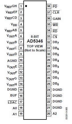
Pinout

  Connection Diagram


Specifications

VDD to GND                                                   0.3 V to +7 V
Digital Input Voltage to GND                 0.3 V to VDD + 0.3 V
Digital Output Voltage to GND              0.3 V to VDD + 0.3 V
Reference Input Voltage to GND           0.3 V to VDD + 0.3 V
VOUT to GND                                      0.3 V to VDD + 0.3 V
Operating Temperature Range
     Industrial (B Version)                         40°C to +105°C
Storage Temperature Range                   65°C to +150°C
Junction Temperature                                                 150°C
38-Lead TSSOP Package
     Power Dissipation                          (TJ max − TA)/ JA mW
     JA Thermal Impedance                                     98.3°C/W
     JC Thermal Impedance                                       8.9°C/W
40-Lead LFCSP Package
     Power Dissipation                           (TJ max − TA)/ JA mW
     JA Thermal Impedance (3-layerboard)               29.6°C/W
Lead Temperature, Soldering (10 sec)                           300°C
     IR Reflow, Peak Temperature 220                                  °C


Description

The AD5346/AD5347/AD53481 are octal 8-, 10-, and 12-bit DACs, operating from a 2.5 V to 5.5 V supply. These devices incorporate an on-chip output buffer that can drive the output to both supply rails, and also allow a choice of buffered or unbuffered reference input.

The AD5346/AD5347/AD5348 have a parallel interface. CS selects the device and data is loaded into the input registers on the rising edge of WR. A readback feature allows the internal DAC registers to be read back through the digital port. The GAIN pin on these devices allows the output range to be set at 0 V to VREF or 0 V to 2 × VREF.

Input data to the DACs is double-buffered, allowing simultaneous update of multiple DACs in a system using theLDAC pin.

An asynchronous CLR input is also provided, which resets the contents of the input register and the DAC register to all zeros. These devices also incorporate a power-on reset circuit that ensures that the DAC output powers on to 0 V and remains there until valid data is written to the device.

All three parts are pin compatible, which allows users to select the amount of resolution appropriate for their application without redesigning their circuit board.


Customers Who Bought This Item Also Bought

Margin,quality,low-cost products with low minimum orders. Secure your online payments with SeekIC Buyer Protection.
Static Control, ESD, Clean Room Products
Boxes, Enclosures, Racks
RF and RFID
Tapes, Adhesives
803
Audio Products
View more