AD5332

Features: `AD5332: Dual 8-Bit DAC in 20-Lead TSSOP`AD5333: Dual 10-Bit DAC in 24-Lead TSSOP`AD5342: Dual 12-Bit DAC in 28-Lead TSSOP`AD5343: Dual 12-Bit DAC in 20-Lead TSSOP`Low Power Operation: 230 A @ 3 V, 300 A @ 5 V via PD Pin`Power-Down to 80 nA @ 3 V, 200 nA @ 5 V`2.5 V to 5.5 V Power Supply...

product image

AD5332 Picture
SeekIC No. : 004269127 Detail

AD5332: Features: `AD5332: Dual 8-Bit DAC in 20-Lead TSSOP`AD5333: Dual 10-Bit DAC in 24-Lead TSSOP`AD5342: Dual 12-Bit DAC in 28-Lead TSSOP`AD5343: Dual 12-Bit DAC in 20-Lead TSSOP`Low Power Operation: 230...

floor Price/Ceiling Price

Part Number:
AD5332
Supply Ability:
5000

Price Break

  • Qty
  • 1~5000
  • Unit Price
  • Negotiable
  • Processing time
  • 15 Days
Total Cost: $ 0.00

SeekIC Buyer Protection PLUS - newly updated for 2013!

  • Escrow Protection.
  • Guaranteed refunds.
  • Secure payments.
  • Learn more >>

Month Sales

268 Transactions

Rating

evaluate  (4.8 stars)

Upload time: 2024/6/7

Payment Methods

All payment methods are secure and covered by SeekIC Buyer Protection PLUS.

Notice: When you place an order, your payment is made to SeekIC and not to your seller. SeekIC only pays the seller after confirming you have received your order. We will also never share your payment details with your seller.
Product Details

Description


Features:

`AD5332: Dual 8-Bit DAC in 20-Lead TSSOP
`AD5333: Dual 10-Bit DAC in 24-Lead TSSOP
`AD5342: Dual 12-Bit DAC in 28-Lead TSSOP
`AD5343: Dual 12-Bit DAC in 20-Lead TSSOP
`Low Power Operation: 230 A @ 3 V, 300 A @ 5 V via PD Pin
`Power-Down to 80 nA @ 3 V, 200 nA @ 5 V
`2.5 V to 5.5 V Power Supply
`Double-Buffered Input Logic
`Guaranteed Monotonic by Design Over All Codes
`Buffered/Unbuffered Reference Input Options
`Output Range: 0VREF or 02 VREF
`Power-On Reset to Zero Volts
`Simultaneous Update of DAC Outputs via LDAC Pin
`Asynchronous CLR Facility
`Low Power Parallel Data Interface
`On-Chip Rail-to-Rail Output Buffer Amplifiers
`Temperature Range: 40 to +105


Application

·Portable Battery-Powered Instruments
·Digital Gain and Offset Adjustment
·Programmable Voltage and Current Sources
·Programmable Attenuators
·Industrial Process Control


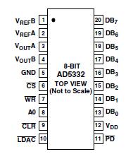
Pinout

  Connection Diagram

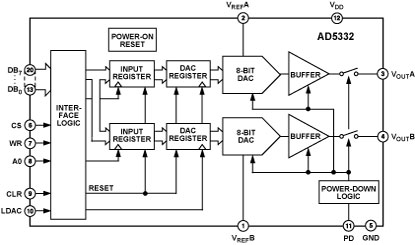
AD5332 Diagram


Specifications

VDD to GND . . . . . . . . . . . . . . . . . . . . . . . . . . 0.3 V to +7 V
Digital Input Voltage to GND . . . . . . . 0.3 V to VDD + 0.3 V
Digital Output Voltage to GND . . . . . 0.3 V to VDD + 0.3 V
Reference Input Voltage to GND . . . . 0.3 V to VDD + 0.3 V
VOUT to GND . . . . . . . . . . . . . . . . . . . 0.3 V to VDD + 0.3 V
Operating Temperature Range
Industrial (B Version) . . . . . . . . . . . . . 40°C to +105°C
Storage Temperature Range . . . . . . . . . .65°C to +150°C
Junction Temperature . . . . . . . . . . . . . . . . . . . . . . . .. 150°C
TSSOP Package
Power Dissipation . . . . . . . . . . . . . .(TJ max TA)/JA mW
JA Thermal Impedance (20-Lead TSSOP) . . . . . 143°C/W
JA Thermal Impedance (24-Lead TSSOP) . . . . . 128°C/W
JA Thermal Impedance (28-Lead TSSOP) . . . . 97.9°C/W
JC Thermal Impedance (20-Lead TSSOP) . . . . . . 45°C/W
JC Thermal Impedance (24-Lead TSSOP) . . . . . . 42°C/W
JC Thermal Impedance (28-Lead TSSOP) . . . . . . 14°C/W
Reflow Soldering
Peak Temperature . . . . . . . . . . . . . . . . . . . . 220 +5/0°C
Time at Peak Temperature . . . . . . . . . . . . 10 sec to 40 sec

*Stresses above those listed under Absolute Maximum Ratings may cause permanent damage to the device. This is a stress rating only; functional operation of the device at these or any other conditions above those listed in the operational sections of this specification is not implied. Exposure to absolute maximum rating conditions for extended periods may affect device reliability.


Resolution (Bits) 8bit
DAC Update Rate 167kSPS
DAC Settling Time 6s
# DAC Outputs 2
DAC Type Voltage Out
DAC Input Format Par
Output FSR (Uni 2Vref),(Uni Vref)
Ref Int/Ext Ext
Supply Vnom Single(+2.7),Single(+3),Single(+3.3),Single(+5)
Pwr Diss 1.8mW
Package SOP


Description

The AD5332/AD5333/AD5342/AD5343 are dual 8-, 10-, and 12-bit DACs. They operate from a 2.5 V to 5.5 V supply consuming just 230 A at 3 V, and feature a power-down pin,PD that further reduces the current to 80 nA. These devices incorporate an on-chip output buffer that can drive the output to both supply rails, while the AD5333 and AD5342 allow a choice of buffered or unbuffered reference input.

The AD5332/AD5333/AD5342/AD5343 have a parallel interface.CS selects the device and data is loaded into the input registers on the rising edge of WR.

The GAIN pin on the AD5333 and AD5342 allows the output range to be set at 0 V to VREF or 0 V to 2 * VREF.

Input data to the DACs is double-buffered, allowing simultaneous update of multiple DACs in a system using theLDAC pin.

An asynchronousCLR input is also provided, which resets the contents of the Input Register and the DAC Register to all zeros. These devices also incorporate a power-on reset circuit that ensures that the DAC output powers on to 0 V and remains there until valid data is written to the device.

The AD5332/AD5333/AD5342/AD5343 are available in Thin Shrink Small Outline Packages (TSSOP).


Customers Who Bought This Item Also Bought

Margin,quality,low-cost products with low minimum orders. Secure your online payments with SeekIC Buyer Protection.
Optical Inspection Equipment
Transformers
Audio Products
Semiconductor Modules
Cable Assemblies
View more