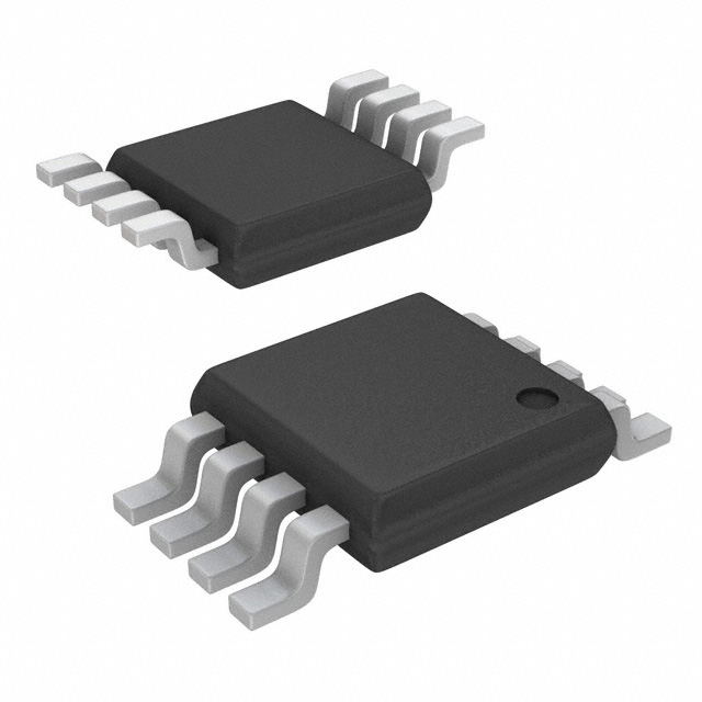
Features: AD5303: Two Buffered 8-Bit DACs in One Package
AD5313: Two Buffered 10-Bit DACs in One Package
AD5323: Two Buffered 12-Bit DACs in One Package
16-Lead TSSOP PackageMicropower Operation: 300 A @ 5 V (IncludingReference Current)Power-Down to 200 nA @ 5 V, 50 nA @ 3 V+2.5 V to +5.5 V Power SupplyDouble-Buffered Input LogicGuaranteed Monotonic By Design Over All CodesBuffered/Unbuffered Reference Input OptionsOutput Range: 0VREF or 02 VREFPower-On-Reset to Zero VoltsSDO Daisy-Chaining OptionSimultaneous Update of DAC Outputsvia LDAC PinAsynchronous CLR FacilityLow Power Serial Interface with Schmitt-TriggeredInputsOn-Chip Rail-to-Rail OutputBuffer Amplifiers
ApplicationPortable Battery Powered InstrumentsDigital Gain and Offset AdjustmentProgrammable Voltage and Current SourcesProgrammable AttenuatorsPinout Specifications(TA = +25 unless otherwise noted)
VDD to GND . . . . . . . . . . . . . . . . . . . . . . . . . . 0.3 V to +7 V
Digital Input Voltage to GND . . . . . . . 0.3 V to VDD + 0.3 V
Digital Output Voltage to GND . . . . . 0.3 V to VDD + 0.3 V
Reference Input Voltage to GND . . . . 0.3 V to VDD + 0.3 V
VOUTA, VOUTB to GND . . . . . . . . . . . 0.3 V to VDD + 0.3 V
Operating Temperature Range
Industrial (B Version) . . . . . . . . . . . . . . . 40°C to +105°C
Storage Temperature Range . . . . . . . . . . . . 65°C to +150°C
Junction Temperature (TJ Max) . . . . . . . . . . . . . . . . .+150°C
16-Lead TSSOP Package
Power Dissipation . . . . . . . . . . . . . . . . . . (TJ Max TA)/JA
JA Thermal Impedance . . . . . . . . . . . . . . . . . . . . 160°C/W
Lead Temperature, Soldering
Vapor Phase (60 sec) . . . . . . . . . . . . . . . . . . . . . .+215°C
Infrared (15 sec) . . . . . . . . . . . . . . . . . . . . . . . . . .+220°CDescriptionThe AD5303/AD5313/AD5323 are dual 8-, 10- and 12-bitbuffered voltage output DACs in a 16-lead TSSOP package thatoperate from a single +2.5 V to +5.5 V supply consuming 230 Aat 3 V. Their on-chip output amplifiers allow the outputs toswing rail-to-rail with a slew rate of 0.7 V/s. The AD5303/AD5313/AD5323 utilize a versatile 3-wire serial interface thatoperates at clock rates up to 30 MHz and is compatible withstandard SPI™, QSPI, MICROWIRE™ and DSP interfacestandards.
The references for the two DACs AD5303/AD5313/AD5323 are derived from two referencepins (one per DAC). These reference inputs may be configuredas buffered or unbuffered inputs. The parts incorporate a poweron-reset circuit that ensures that the DAC outputs power-up to0 V and remain there until a valid write to the device takes place.There is also an asynchronous active low CLR pin that clearsboth DACsto 0 V. The outputs of both DACs may be updatedsimultaneously using the asynchronous LDAC input. Theparts contain a power-down feature that reduces the currentconsumption of the devices to 200 nA at 5 V (50 nA at 3 V) andprovides software-selectable output loads while in power-downmode. The parts may also be used in daisy-chaining applicationsusing the SDO pin.
The low power consumption of these parts AD5303/AD5313/AD5323 in normal operationmake them ideally suited to portable battery operated equipment.The power consumption is 1.5 mW at 5 V, 0.7 mW at3 V, reducing to 1 W in power-down mode.

 AD5323* Data Sheet

 A @ 5 V (IncludingReference Current)Power-Down to 200 nA @ 5 V, 50 nA @ 3 V+2.5 V to +5.5 V Power SupplyDouble-Buffered Input LogicGuaranteed Monotonic By Design Over All CodesBuffered/Unbuffered Reference Input OptionsOutput Range: 0VREF or 02 VREFPower-On-Reset to Zero VoltsSDO Daisy-Chaining OptionSimultaneous Update of DAC Outputsvia LDAC PinAsynchronous CLR FacilityLow Power Serial Interface with Schmitt-TriggeredInputsOn-Chip Rail-to-Rail OutputBuffer Amplifiers


