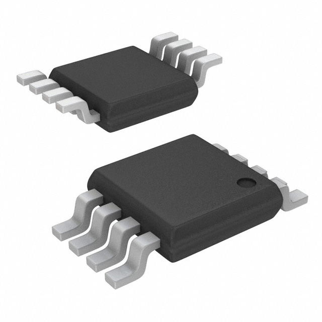
Features: AD5301: Buffered Voltage Output 8-Bit DAC
AD5311: Buffered Voltage Output 10-Bit DAC
AD5321: Buffered Voltage Output 12-Bit DAC
6-Lead SOT-23 and 8-Lead mSOIC PackagesMicropower Operation: 120 mA @ 3 V2-Wire (I2C® Compatible) Serial InterfaceData Readback Capability+2.5 V to +5.5 V Power SupplyGuaranteed Monotonic By Design Over All CodesPower-Down to 50 nA @ 3 VReference Derived from Power SupplyPower-On-Reset to Zero VoltsOn-Chip Rail-to-Rail Output Buffer AmplifierThree Power-Down Functions ApplicationPortable Battery Powered Instruments
Digital Gain and Offset Adjustment
Programmable Voltage and Current Sources
Programmable AttenuatorsPinout
 SpecificationsVDD to GND . . . . . . . . . . . . . . . . . . . . . . . . . . . 0.3 V to +7 V
SCL, SDA to GND . . . . . . . . . . . . . . . . 0.3 V to VDD + 0.3 V
PD, A1, A0 to GND . . . . . . . . . . . . . . . 0.3 V to VDD + 0.3 V
VOUT to GND . . . . . . . . . . . . . . . . . . . . 0.3 V to VDD + 0.3 V
Operating Temperature Range
Industrial (B Version) . . . . . . . . . . . . . . . . 40 to +105
Storage Temperature Range . . . . . . . . . . . . . 65 to +150
Junction Temperature (TJ max) . . . . . . . . . . . . . . . . . . .+150
SOT-23 Package
Power Dissipation . . . . . . . . . . . . . . . . . . . (TJ max TA)/qJA
qJA Thermal Impedance . . . . . . . . . . . . . . . . . . . . 229.6/W
mSOIC Package
Power Dissipation . . . . . . . . . . . . . . . . . . . (TJ max TA)/qJA
qJA Thermal Impedance . . . . . . . . . . . . . . . . . . . . . 206/W
Lead Temperature, Soldering
Vapor Phase (60 sec) . . . . . . . . . . . . . . . . . . . . . . . . +215
Infrared (15 sec) . . . . . . . . . . . . . . . . . . . . . . . . . . . . +220
| Resolution (Bits) |
12bit |
| DAC Update Rate |
125kSPS |
| DAC Settling Time |
8s |
| # DAC Outputs |
1 |
| DAC Type |
Voltage Out |
| DAC Input Format |
I2C/Ser 2-wire,Ser |
| Output FSR |
(Uni Vdd) |
| Ref Int/Ext |
Int |
| Supply Vnom |
Single(+2.5),Single(+2.7),Single(+3),Single(+3.3),Single(+5) |
| Pwr Diss |
1.4mW |
| Package |
SOP,SOT |
DescriptionThe AD5301/AD5311/AD5321 are single 8-, 10- and 12-bitbuffered voltage-output DACs that operate from a single +2.5 Vto +5.5 V supply consuming 120 mA at 3 V. The on-chip outputamplifier allows rail-to-rail output swing with a slew rate of0.7 V/ms. It uses a 2-wire (I2C compatible) serial interface thatoperates at clock rates up to 400 kHz. Multiple devices canshare the same bus.
The reference for the DAC AD5301/AD5311/AD5321 is derived from the power supplyinputs and thus gives the widest dynamic output range. Theseparts incorporate a power-on-reset circuit, which ensures thatthe DAC output powers-up to zero volts and remains there untila validwrite takes place. The parts contain a power-down featurewhich reduces the current consumption of the device to 50 nAat 3 V and provides software-selectable output loads while inpower-down mode.
The low power consumption of AD5301/AD5311/AD5321 in normal operation make theseDACs ideally suited to portable battery-operated equipment.The power consumption is 0.75 mW at 5 V, 0.36 mW at 3 Vreducing to 1 mW in all power-down modes.
The AD5301/AD5311/AD5321* are single 8-/10-/12-bit, buffered, voltage-output DACs that operate from a single 2.5 V to 5.5 V supply, consuming 120 A at 3 V. The on-chip output amplifier allows

 AD5321 Data Sheet


