AD5305

Features: `AD5305: 4 Buffered 8-Bit DACs in 10-Lead MSOP`A Version: ±1 LSB INL, B Version: ±0.625 LSB INL`AD5315: 4 Buffered 10-Bit DACs in 10-Lead MSOP`A Version: ±4 LSB INL, B Version: ±2.5 LSB INL`AD5325: 4 Buffered 12-Bit DACs in 10-Lead MSOP`A Version: ±16 LSB INL, B Version: ±10 LSB INL`Low ...

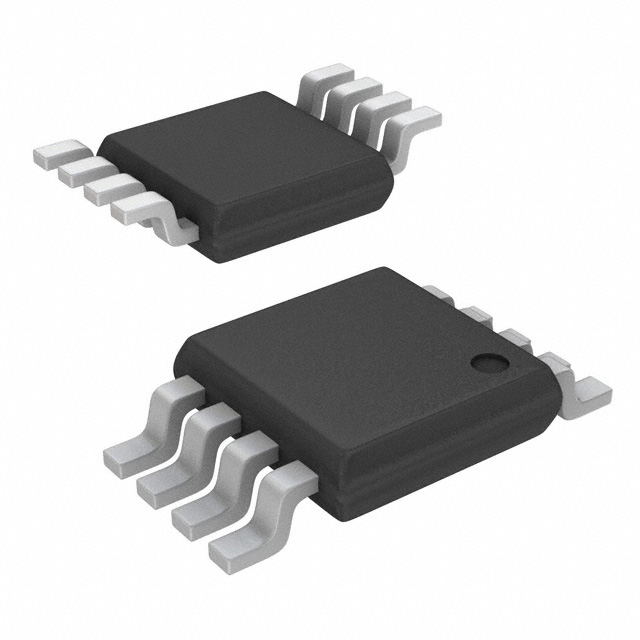
product image

AD5305 Picture
SeekIC No. : 004269044 Detail

AD5305: Features: `AD5305: 4 Buffered 8-Bit DACs in 10-Lead MSOP`A Version: ±1 LSB INL, B Version: ±0.625 LSB INL`AD5315: 4 Buffered 10-Bit DACs in 10-Lead MSOP`A Version: ±4 LSB INL, B Version: ±2.5 LSB IN...

floor Price/Ceiling Price

Part Number:
AD5305
Supply Ability:
5000

Price Break

  • Qty
  • 1~5000
  • Unit Price
  • Negotiable
  • Processing time
  • 15 Days
Total Cost: $ 0.00

SeekIC Buyer Protection PLUS - newly updated for 2013!

  • Escrow Protection.
  • Guaranteed refunds.
  • Secure payments.
  • Learn more >>

Month Sales

268 Transactions

Rating

evaluate  (4.8 stars)

Upload time: 2024/5/27

Payment Methods

All payment methods are secure and covered by SeekIC Buyer Protection PLUS.

Notice: When you place an order, your payment is made to SeekIC and not to your seller. SeekIC only pays the seller after confirming you have received your order. We will also never share your payment details with your seller.
Product Details

Description


Features:

`AD5305: 4 Buffered 8-Bit DACs in 10-Lead MSOP
`A Version: ±1 LSB INL, B Version: ±0.625 LSB INL
`AD5315: 4 Buffered 10-Bit DACs in 10-Lead MSOP
`A Version: ±4 LSB INL, B Version: ±2.5 LSB INL
`AD5325: 4 Buffered 12-Bit DACs in 10-Lead MSOP
`A Version: ±16 LSB INL, B Version: ±10 LSB INL
`Low Power Operation: 500 A @ 3 V, 600 A @ 5 V
`2-Wire (I2C® Compatible) Serial Interface
`2.5 V to 5.5 V Power Supply
`Guaranteed Monotonic by Design over All Codes
`Power-Down to 80 nA @ 3 V, 200 nA @ 5 V
`Three Power-Down Modes
`Double-Buffered Input Logic
`Output Range: 0 V to VREF
`Power-On Reset to 0 V
`Simultaneous Update of Outputs (LDAC Function)
`Software Clear Facility
`Data Readback Facility
`On-Chip Rail-to-Rail Output Buffer Amplifiers
`Temperature Range 40 to +105


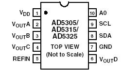
Pinout

  Connection Diagram

AD5305 Diagram


Specifications

VDD to GND . . . . . . . . . . . . . . . . . . . . . . . . . 0.3 V to +7 V
SCL, SDA to GND . . . . . . . . . . . . . . . . 0.3 V to VDD + 0.3 V
A0 to GND . . . . . . . . . . . . . . . . . . . . . 0.3 V to VDD + 0.3 V
Reference Input Voltage to GND . . . . 0.3 V to VDD + 0.3 V
VOUT AD to GND . . . . . . . . . . . . . . . 0.3 V to VDD + 0.3 V
Operating Temperature Range
Industrial (A, B Version) . . . . . . . . . . . . 40°C to +105°C
Storage Temperature Range . . . . . . . . . 65°C to +150°C
Junction Temperature (TJ max) . . . . . . . . . . . . . . . . . 150°C
MSOP
Power Dissipation . . . . . . . . . . . . . . . . .. . (TJ max TA)/JA
JA Thermal Impedance . . . . . . . . . . . . . . . . . . . . 206°C/W
JC Thermal Impedance . . . . . . . . . . . . . . . . . .. . . . 44°C/W
Reflow Soldering
Peak Temperature . . . . . . . . . . . . . . . . . . . . . . . . . . . 220°C
Time at Peak Temperature . . . . . . . . . . . . . 10 sec to 40 sec


Resolution (Bits) 8bit
DAC Update Rate 167kSPS
DAC Settling Time 6s
# DAC Outputs 4
DAC Type Voltage Out
DAC Input Format I2C/Ser 2-wire,Ser
Output FSR (Uni Vref)
Ref Int/Ext Ext
Supply Vnom Single(+2.5),Single(+2.7),Single(+3),Single(+3.3),Single(+5)
Pwr Diss (Max) 5mW
Package SOP


Description

The AD5305/AD5315/AD5325 are quad 8-, 10-, and 12-bit buffered voltage output DACs in a 10-lead MSOP that operate from a single 2.5 V to 5.5 V supply, consuming 500 µA at 3 V. Their on-chip output amplifiers allow rail-to-rail output swing with a slew rate of 0.7 V/µs. A 2-wire serial interface, which operates at clock rates up to 400 kHz, is used. This interface is SMBus compatible at VDD < 3.6 V. Multiple devices can be placed on the same bus.

The references for the four DACs AD5305 are derived from one reference pin. The outputs of all DACs may be updated simultaneously using the software LDAC function. The parts incorporate a power-on reset circuit, which ensures that the DAC outputs power up to 0 V and remain there until a valid write takes place to the device. There is also a software clear function that resets all input and DAC registers to 0 V.

The parts of AD5305 contain a power-down feature that reduces the current consumption of the devices to 200 nA @ 5 V (80 nA @ 3 V). The low power consumption of these parts in normal operation makes them ideally suited to portable battery-operated equipment. The power consumption is 3 mW at 5 V, 1.5 mW at 3 V, reducing to 1 µW in power-down mode.


Customers Who Bought This Item Also Bought

Margin,quality,low-cost products with low minimum orders. Secure your online payments with SeekIC Buyer Protection.
LED Products
Discrete Semiconductor Products
Semiconductor Modules
Optoelectronics
Inductors, Coils, Chokes
Undefined Category
View more