Features: AD5303: Two Buffered 8-Bit DACs in One Package
AD5313: Two Buffered 10-Bit DACs in One Package
AD5323: Two Buffered 12-Bit DACs in One Package
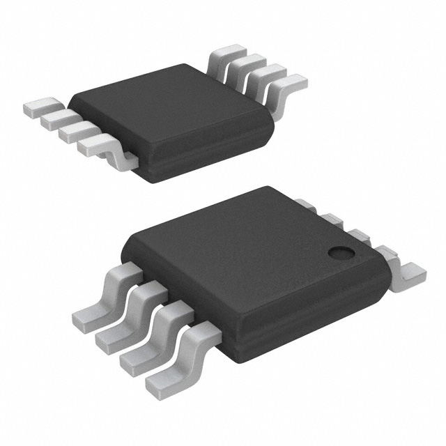
16-Lead TSSOP PackageMicropower Operation: 300 A @ 5 V (IncludingReference Current)Power-Down to 200 nA @ 5 V, 50 nA @ 3 V+2.5 V to +5.5 V Power SupplyDouble-Buffered Input LogicGuaranteed Monotonic By Design Over All CodesBuffered/Unbuffered Reference Input OptionsOutput Range: 0VREF or 02 VREFPower-On-Reset to Zero VoltsSDO Daisy-Chaining OptionSimultaneous Update of DAC Outputsvia LDAC PinAsynchronous CLR FacilityLow Power Serial Interface with Schmitt-TriggeredInputsOn-Chip Rail-to-Rail OutputBuffer Amplifiers
Pinout
 Specifications(TA = +25 unless otherwise noted)
VDD to GND . . . . . . . . . . . . . . . . . . . . . . . . . . 0.3 V to +7 V
Digital Input Voltage to GND . . . . . . . 0.3 V to VDD + 0.3 V
Digital Output Voltage to GND . . . . . 0.3 V to VDD + 0.3 V
Reference Input Voltage to GND . . . . 0.3 V to VDD + 0.3 V
VOUTA, VOUTB to GND . . . . . . . . . . . 0.3 V to VDD + 0.3 V
Operating Temperature Range
Industrial (B Version) . . . . . . . . . . . . . . . 40°C to +105°C
Storage Temperature Range . . . . . . . . . . . . 65°C to +150°C
Junction Temperature (TJ Max) . . . . . . . . . . . . . . . . .+150°C
16-Lead TSSOP Package
Power Dissipation . . . . . . . . . . . . . . . . . . (TJ Max TA)/JA
JA Thermal Impedance . . . . . . . . . . . . . . . . . . . . 160°C/W
Lead Temperature, Soldering
Vapor Phase (60 sec) . . . . . . . . . . . . . . . . . . . . . .+215°C
Infrared (15 sec) . . . . . . . . . . . . . . . . . . . . . . . . . .+220°C
| Resolution (Bits) |
8bit |
| DAC Update Rate |
167kSPS |
| DAC Settling Time |
6s |
| # DAC Outputs |
2 |
| DAC Type |
Voltage Out |
| DAC Input Format |
Ser,SPI |
| Output FSR |
(Uni 2Vref),(Uni Vref) |
| Ref Int/Ext |
Ext |
| Supply Vnom |
Single(+2.5),Single(+2.7),Single(+3),Single(+3.3),Single(+5) |
| Pwr Diss |
2.5mW |
| Package |
SOP |
DescriptionThe AD5303/AD5313/AD5323 are dual 8-, 10- and 12-bitbuffered voltage output DACs in a 16-lead TSSOP package thatoperate from a single +2.5 V to +5.5 V supply consuming 230 Aat 3 V. Their on-chip output amplifiers allow the outputs toswing rail-to-rail with a slew rate of 0.7 V/s. The AD5303/AD5313/AD5323 utilize a versatile 3-wire serial interface thatoperates at clock rates up to 30 MHz and is compatible withstandard SPI™, QSPI, MICROWIRE™ and DSP interfacestandards.
The references for the two DACs are derived from two referencepins (one per DAC). These reference inputs of AD5303 may be configuredas buffered or unbuffered inputs. The parts incorporate a poweron-reset circuit that ensures that the DAC outputs power-up to0 V and remain there until a valid write to the device takes place.There is also an asynchronous active low CLR pin that clearsboth DACsto 0 V. The outputs of both DACs may be updatedsimultaneously using the asynchronous LDAC input. Theparts contain a power-down feature that reduces the currentconsumption of the devices to 200 nA at 5 V (50 nA at 3 V) andprovides software-selectable output loads while in power-downmode. The parts may also be used in daisy-chaining applicationsusing the SDO pin.
The low power consumption of these parts in normal operationmake them ideally suited to portable battery operated equipment.The power consumption is 1.5 mW at 5 V, 0.7 mW at3 V, reducing to 1 W in power-down mode.

 AD5303 Data Sheet