Features: Low Noise: 0.3 mV p-p 0.1 Hz to 10 Hz
Low Nonlinearity: 0.003% (G = 1)
High CMRR: 120 dB (G = 1000)
Low Offset Voltage: 50 mV
Low Offset Voltage Drift: 0.5 mV/8C
Gain Bandwidth Product: 25 MHz
Pin Programmable Gains of 1, 10, 100, 1000
Input Protection, Power OnPower Off
No External Components Required
Internally Compensated
MIL-STD-883B and Chips Available
16-Lead Ceramic DIP and SOIC Packages and
20-Terminal Leadless Chip Carriers Available
Available in Tape and Reel in Accordance
with EIA-481A Standard
Standard Military Drawing Also AvailablePinout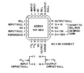 SpecificationsSupply Voltage . . . . . . . . . . . . . . . . . . . . . . . . . . . . . . . . 18V
Internal Power Dissipation . . . . . . . . . . . . . . . . . . . . .450 mW
2
Input Voltage
(Either Input Simultaneously) |VIN| + |VS| . . . . . . . . <36 V
Output Short Circuit Duration . . . . . . . . . . . . . . . . . Indefinite
Storage Temperature Range
(R) . . . . . . . . . . . . . . . . . . . . . . . . . . . . . . 65 C to +125 C
(D, E) . . . . . . . . . . . . . . . . . . . . . . . . . . . 65 C to +150 C
Operating Temperature Range
AD524A/B/C . . . . . . . . . . . . . . . . . . . . . . . . 25 C to +85 C
AD524S . . . . . . . . . . . . . . . . . . . . . . . . . . 55 C to +125 C
Lead Temperature (Soldering 60 secs) . . . . . . . . . . . . +300 C
NOTES
1
Stresses above those listed under Absolute Maximum Ratings may cause permanent damage to the device. This is a stress rating only; functional operation of the device at these or any other conditions above those indicated in the operational section of this specification is not implied. Exposure to absolute maximum rating conditions for extended periods may affect device reliability.
2
Max input voltage specification refers to maximum voltage to which either input terminal may be raised with or without device power applied. For example, with 18 volt supplies max VIN is 18 volts, with zero supply voltage max VIN is 36 volts. DescriptionThe AD524 is a precision monolithic instrumentation amplifier designed for data acquisition applications requiring high accuracy under worst-case operating conditions. An outstanding combination of high linearity, high common mode rejection, low offset voltage drift and low noise makes the AD524 suitable for use in many data acquisition systems.
The AD524 has an output offset voltage drift of less than 25 mV/ C, input offset voltage drift of less than 0.5 mV/ C, CMR above 90dB at unity gain (120 dB at G = 1000) and maximum nonlinearity of 0.003% at G = 1. In addition to the outstanding dc specifications, the AD524 also has a 25 kHz gain bandwidth product (G = 1000). To make it suitable for high speed data acquisition systems the AD524 has an output slew rate of 5 V/ms and settles in 15 ms to 0.01% for gains of 1 to 100.
As a complete amplifier the AD524 does not require any external components for fixed gains of 1, 10, 100 and 1000. For other gain settings between 1 and 1000 only a single resistor is required. The AD524 input is fully protected for both power-on and power-off fault conditions.
The AD524 IC instrumentation amplifier is available in four different versions of accuracy and operating temperature range. The economical "A" grade, the low drift "B" grade and lower drift, higher linearity "C" grade are specified from 25 C to +85 C. The "S" grade guarantees performance to specification over the extended temperature range 55 C to +125 C. Devices are available in 16-lead ceramic DIP and SOIC packages and a
20-terminal leadless chip carrier.

 AD524 Data Sheet